
Composite wafers having bulk-quality semiconductor layers and method of manufacturing thereof
a technology of semiconductor layers and composite wafers, which is applied in the direction of layered products, radiation intensity measurement, transportation and packaging, etc., can solve the problems of limited wafer availability or and achieve the effect of limited wafer availability and high cost of bulk wafers
Patent Information
- Authority / Receiving Office
- US · United States
- Current Assignee / Owner
- Publication Date
- 2008-12-04
- Estimated Expiration
- Not applicable · inactive patent
Smart Images
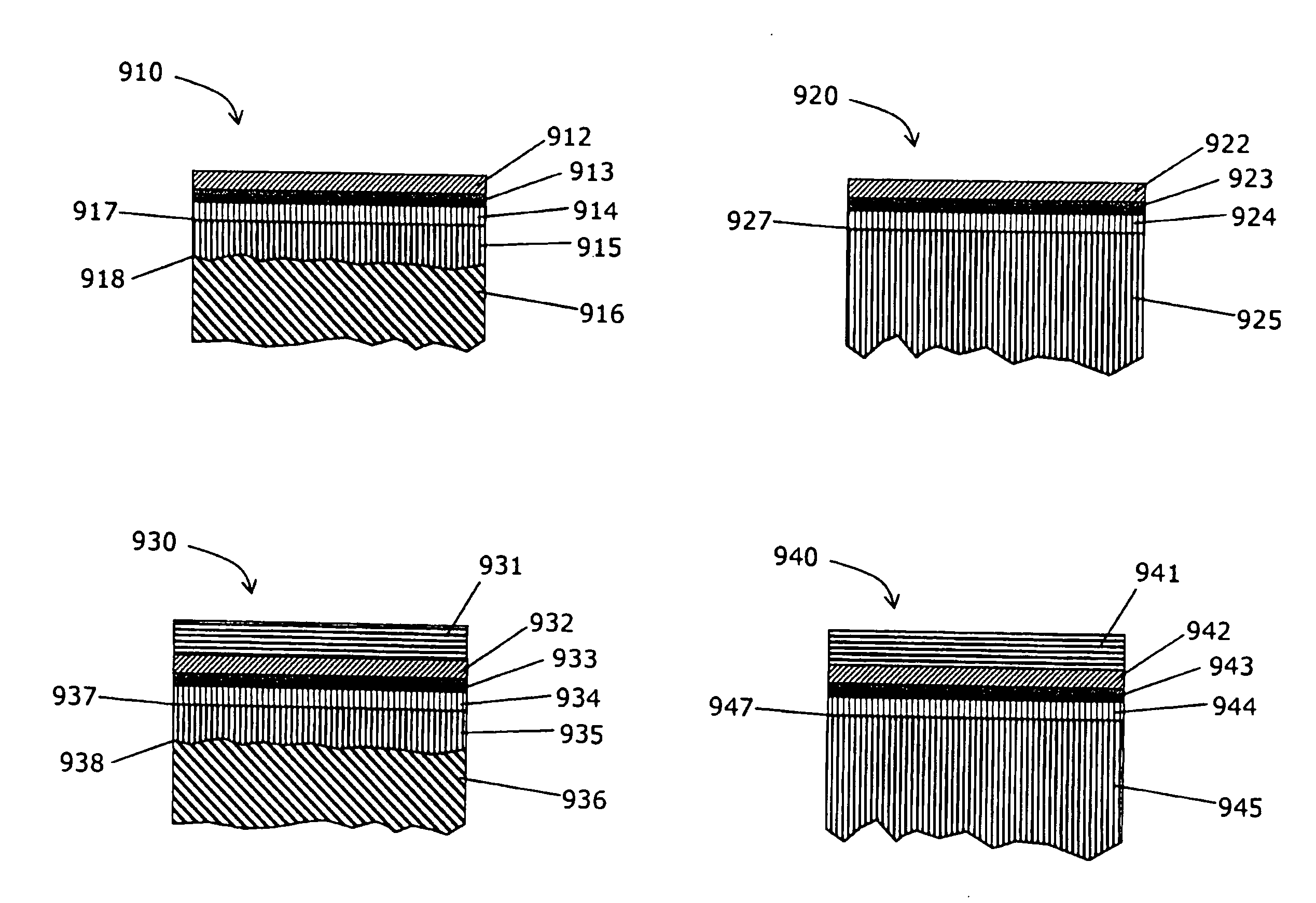
Figure 1 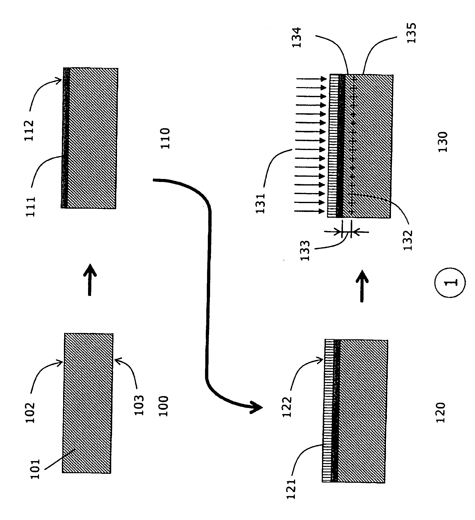
Figure 2 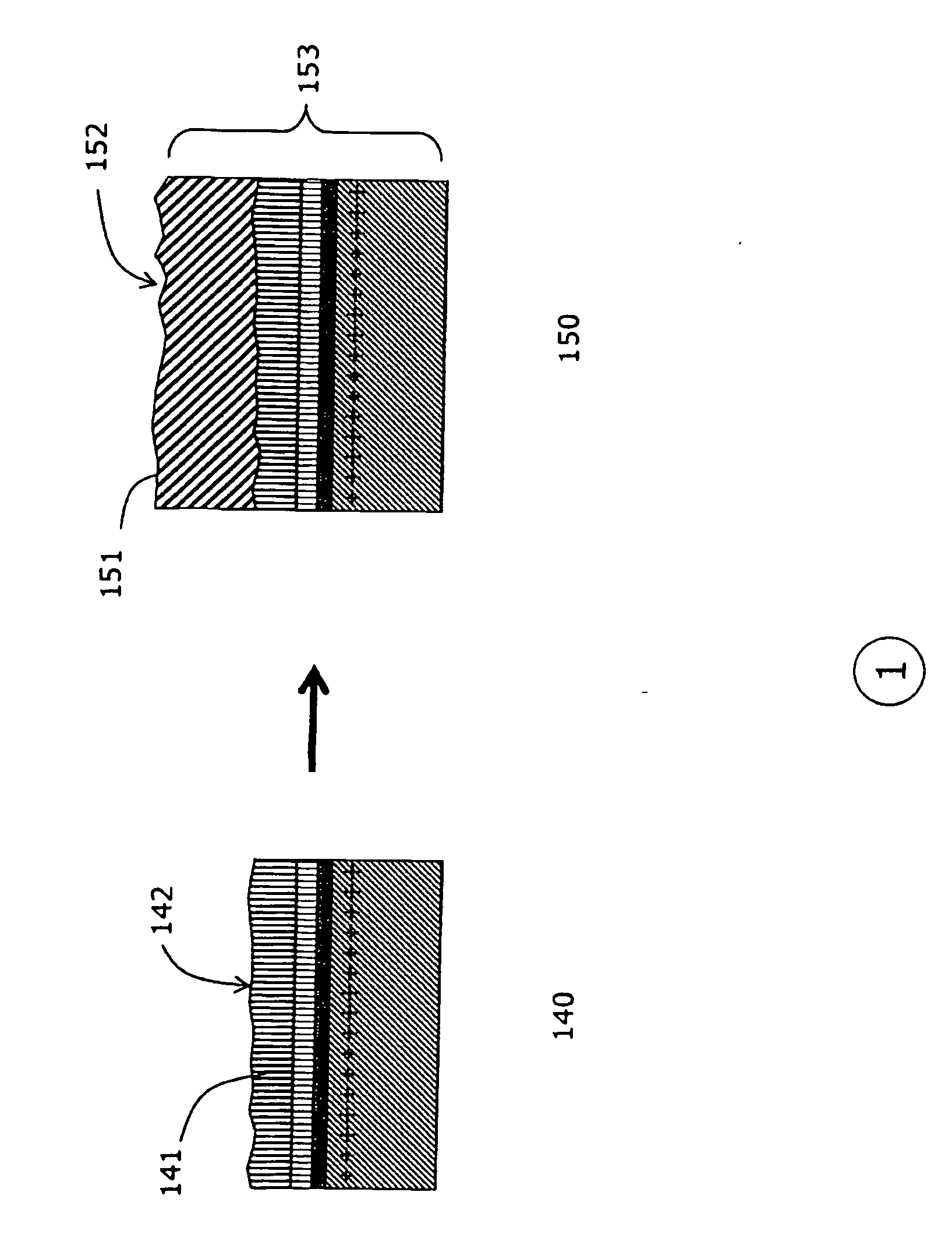
Figure 3
Abstract
Description
RELATED APPLICATIONS
[0001] This application claims benefit of U.S. Provisional Patent Application Serial No. 60 / 881,951 filed Jan. 22, 2007.FIELD OF THE INVENTION
[0002] The present invention relates to the manufacture of bulk-quality semiconductor thin films on synthetic diamond by transferring mentioned semiconductor films from bulk single-crystal semiconductor wafer onto synthetic diamond substrate. The transfer of said semiconductor layer may be repeated so that a multiplicity of diamond substrates with atomically attached semiconductor layers are manufactured from a single bulk semiconductor wafer. More specifically, this invention is related to gallium nitride semiconductor thin films and bulk-grown wafers.BACKGROUND OF THE INVENTION
[0003] Gallium nitride (GaN) films are typically grown using metal-organic chemical vapor deposition (MOCVD) process on one of several available substrates. The historically first and most common substrate material used for growing GaN has been sapphir...
Examples
Embodiment Construction
[0047]The preferred process according to this invention and various embodiments comprise of the following step described below and illustrated in FIGS. 1, 2 and 3. The process flow is given in FIG. 7a.
[0048]The first embodiment of the preferred method is illustrated in FIG. 7a and described more specifically in FIG. 1: In step 100 of FIG. 1, a bulk gallium nitride wafer 101 is provided. The wafer 101 has a planar surface 102 and whose plane is either substantially parallel or slightly inclined with respect to one of the principal crystallographic planes of a single-crystal semiconductor material.
[0049]In the next step 110, the surface 102 of the gallium nitride substrate is prepared for diamond nucleation by depositing a layer 111. This requires high adhesion. Hence, surface 102 is prepared by polishing. The preferred root-mean-square roughness of surface 102 is at least 1 nm. The surface preparation required in this step 110 is equivalent to the one described in the last steps of ...