
Method and structure for domino read bit line and set reset latch
Patent Information
- Authority / Receiving Office
- US · United States
- Current Assignee / Owner
- Publication Date
- 2008-12-04
- Estimated Expiration
- Not applicable · inactive patent
Smart Images
Figure 1 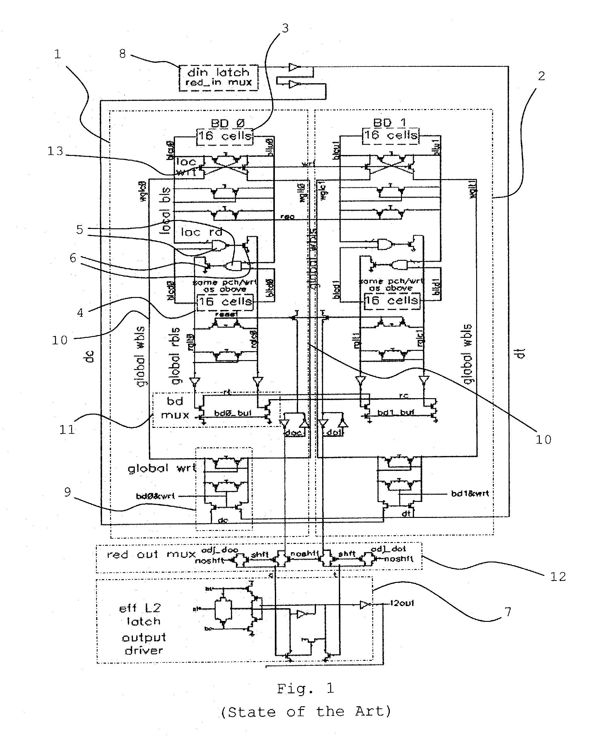
Figure 2 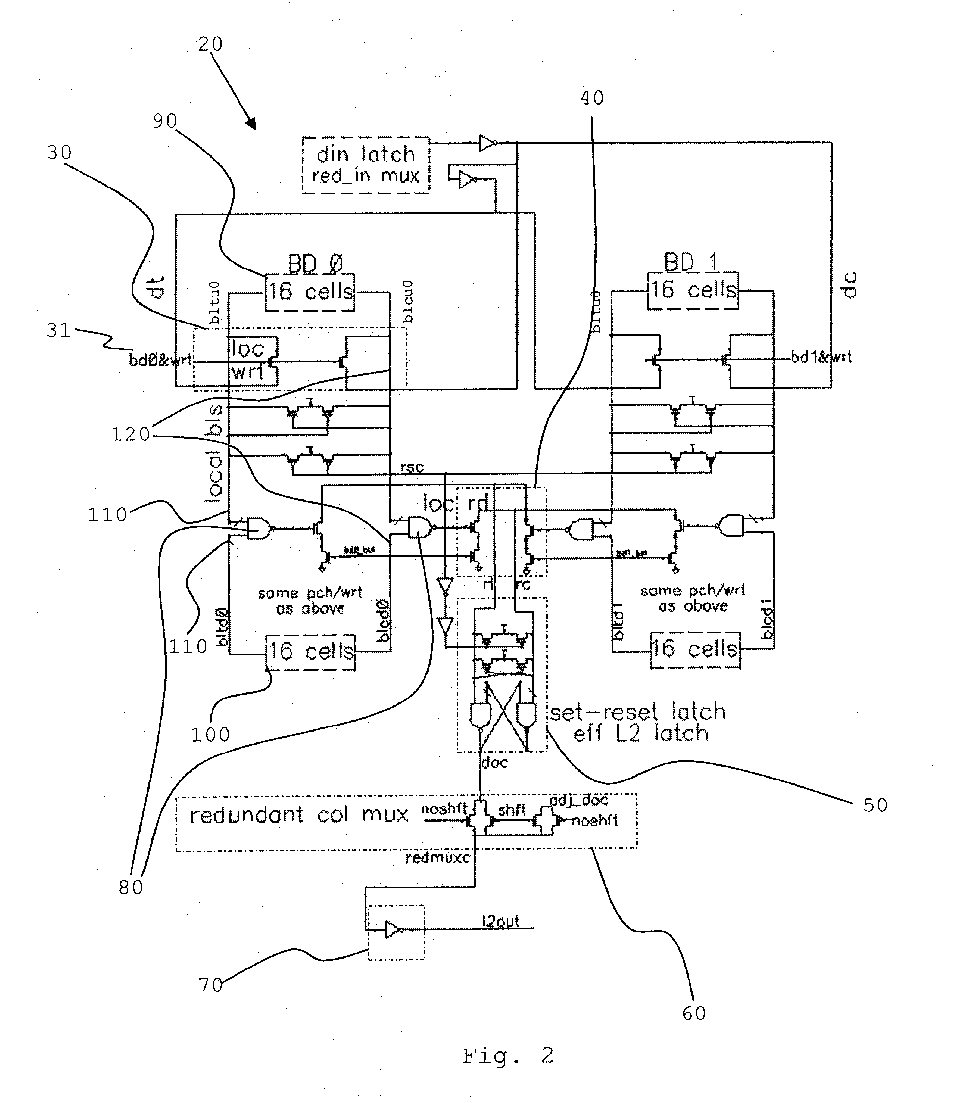
Figure 3
Abstract
Description
CROSS REFERENCES TO RELATED APPLICATION
[0001] This application is related to one European Application No. 07104632.0 filed Mar. 22, 2007FIELD OF THE INVENTION
[0002] The invention relates to a domino read bit line structure in conjunction with a small static random access memory (SRAM) array with thirty-two word lines or less plus a set-reset latch for such a bit line structure, which allows to evaluation of the SRAM array during test.BACKGROUND OF THE INVENTION
[0003] SRAM is a type of semiconductor memory in which the memory retains its contents as long as power remains applied, unlike dynamic random access memory (DRAM) which needs to be periodically refreshed. Each bit in an SRAM is stored in a storage cell comprising four transistors that form two cross-coupled inverters. This storage cell has two stable states which are used to denote ‘0’ and ‘1’. Two additional access transistors serve to control the access to a storage cell during read and write operations. It thus typically take...
Examples
Embodiment Construction
[0022]A bit line structure 20 according to a preferred embodiment is shown in FIG. 2, which achieves a significant reduction in device count as compared to the prior art implementation of FIG. 1. This device reduction is achieved by completely removing the read global bit line structures (rglt0 and rglc0 in FIG. 1) and write global bit line structures (wglc0 and wglt0 in FIG. 1). This is made possible by combining the bit decode multiplexer (11 in FIG. 1) directly into the local evaluation circuitry (80 and 40 in FIG. 2) and by incorporating the column select signal (bd0&wrt in FIG. 1) into the local write control signal of FIG. 2.
[0023]The true and complement local bit lines bltu0 and blcu0 from the upper 3, and bltd0 and blcd0 from the lower group 4 (FIG. 1) and 110 and 120 respectively (FIG. 2) are read in the same manner in both approaches. They are pre-charged high and realize the same capacitive load. This guarantees the same read margin for the array as in the bit line struct...