
Method and structure for textured thermal cut for photovoltaic applications for thin films
Patent Information
- Authority / Receiving Office
- US · United States
- Current Assignee / Owner
- Publication Date
- 2009-03-12
- Estimated Expiration
- Not applicable · inactive patent
Smart Images
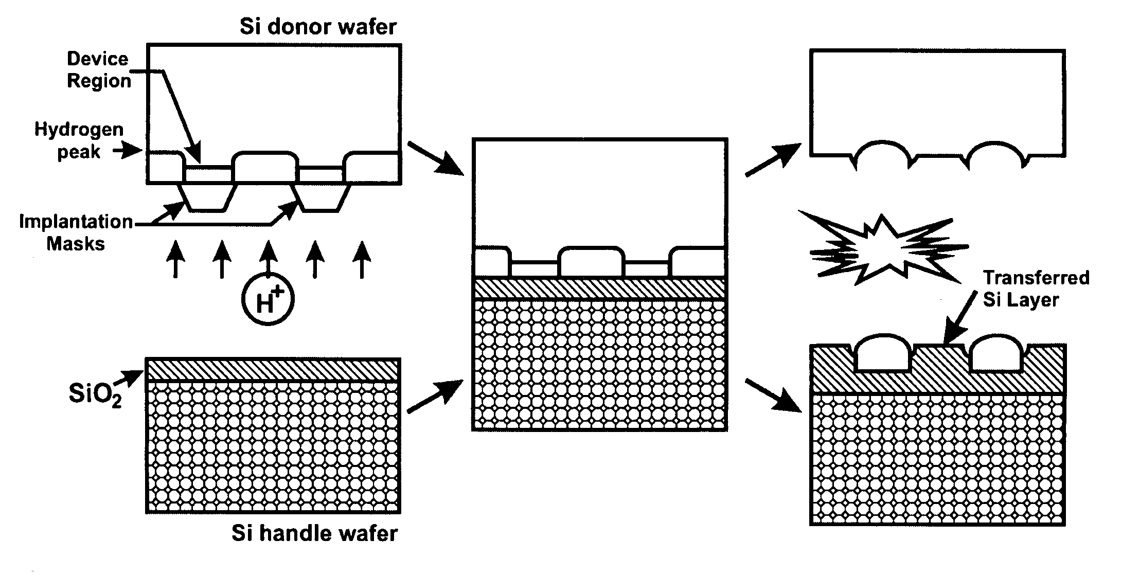
Figure 1 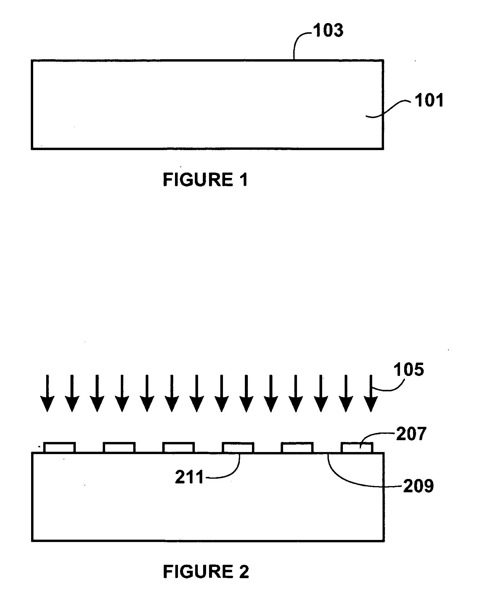
Figure 2 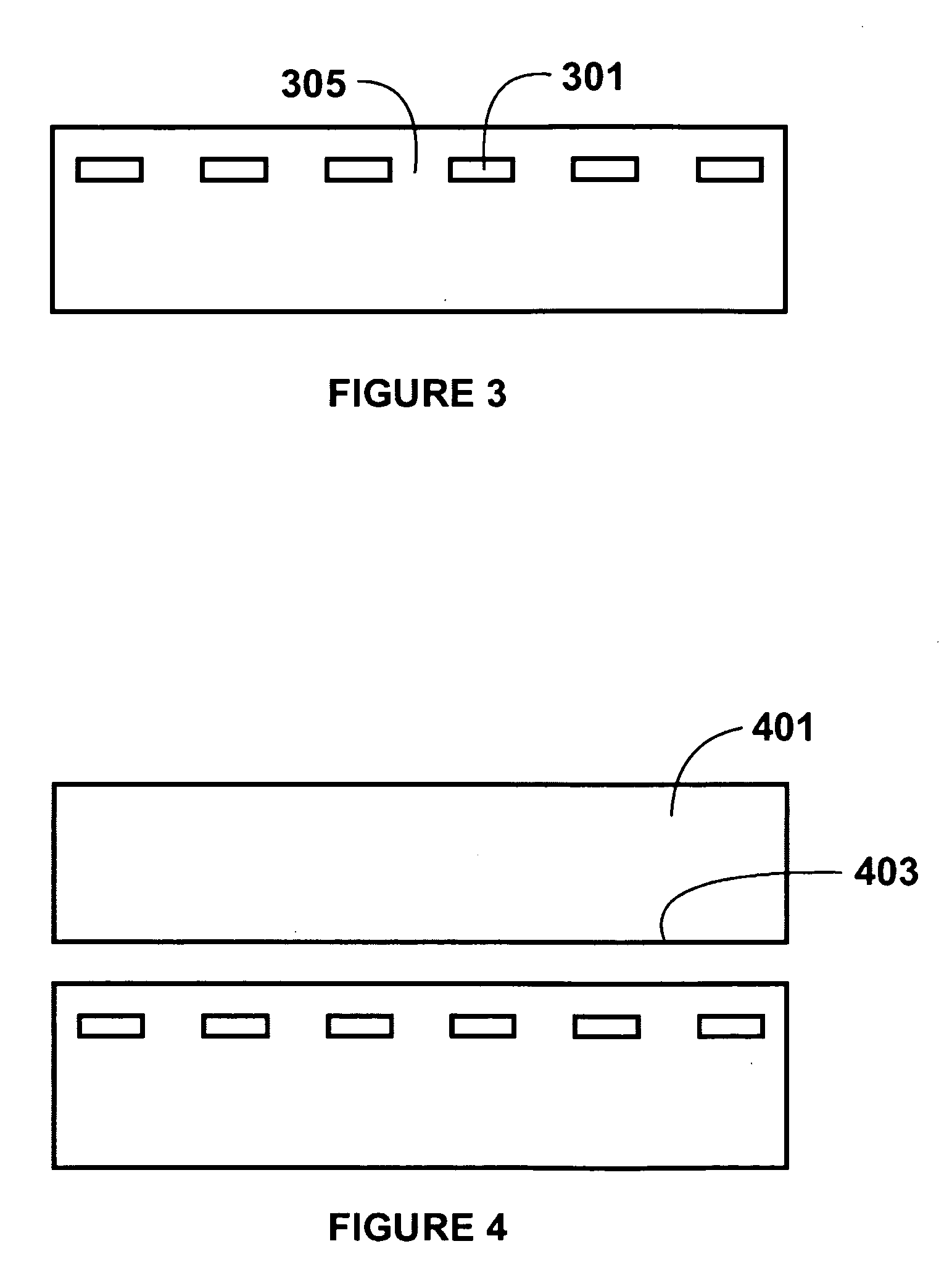
Figure 3
Abstract
Description
CROSS-REFERENCES TO RELATED APPLICATIONS
[0001] This application claims priority to U.S. Provisional Application No. 60 / 971,517 filed Sep. 11, 2007, which is incorporated by reference herein for all purposes.BACKGROUND OF THE INVENTION
[0002] The present invention relates generally to solar energy techniques. In particular, the present invention provides a method and resulting device fabricated from a thermal separation process to form a textured region for photovoltaic applications. More particularly, the present invention provides a method and resulting device for manufacturing the photovoltaic regions with improved light trapping capabilities overlying a substrate member. Such substrate member can be a support member, such as a low grade polysilicon plate, metal plate, glass plate, a combination of these, or the like. Merely by way of example, the invention has been applied to solar panels, commonly termed modules, but it would be recognized that the invention has a much broader rang...
Examples
embodiment
General Method Embodiment
[0017]In a specific embodiment, the present invention provides a method for fabricating a photovoltaic device that can be outlined as follows:
[0018]1. Provide a semiconductor substrate, e.g., single crystal silicon, silicon germanium, Group II / VI, Group III / V;
[0019]2. Form a blocking layer (e.g., mask, block, photo mask) including a plurality of opened regions overlying the surface region of the semiconductor substrate;
[0020]3. Forming a patterned cleave region using an co-implant process including hydrogen species by subjecting at least the hydrogen species to the plurality of opened regions to define a thickness of material to be detached, which is provided between the surface region and the patterned cleave region;
[0021]4. Remove the blocking layer;
[0022]5. Join the surface region of the semiconductor substrate via a glue layer to a support surface region of a support substrate;
[0023]6. Delaminate the thickness of material from a remaining portion of the ...
examples
[0047]To prove the principles and operation of the present invention, we have performed experiments. These experiments are merely examples, which should not unduly limit the scope of the claims herein. One of ordinary skill in the art would recognize many variations, modifications, and alternatives. These experiments are merely for purposes of demonstrating the texturing process in accordance with the present invention. Referring To FIG. 9, we have provided a simplified set of diagrams illustrating our experiment.
[0048]As shown, we provided a method for fabricating a photovoltaic material. As shown, the method includes providing a single crystal silicon semiconductor substrate, which includes surface region. The substrate included a blocking layer overlying the surface region. In a specific embodiment, the blocking layer was photosensitive material that included a plurality of opened regions. Such opened regions are separated by blocking layer according to a specific embodiment. We ...