
Semiconductor Device and Method of Forming Interconnect Structure in Non-Active Area of Wafer
Patent Information
- Authority / Receiving Office
- US · United States
- Current Assignee / Owner
- Publication Date
- 2009-03-26
Smart Images
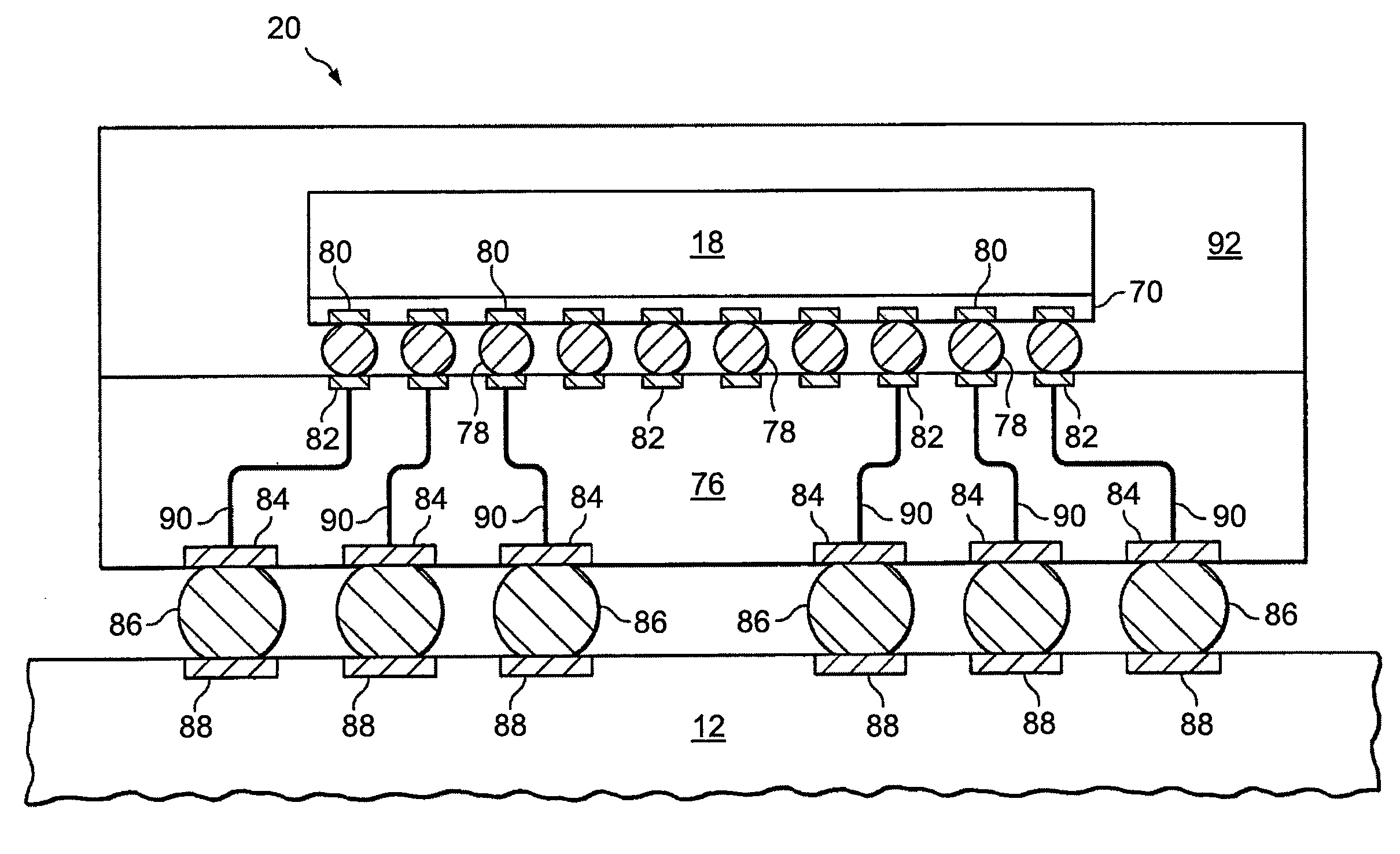
Figure 1 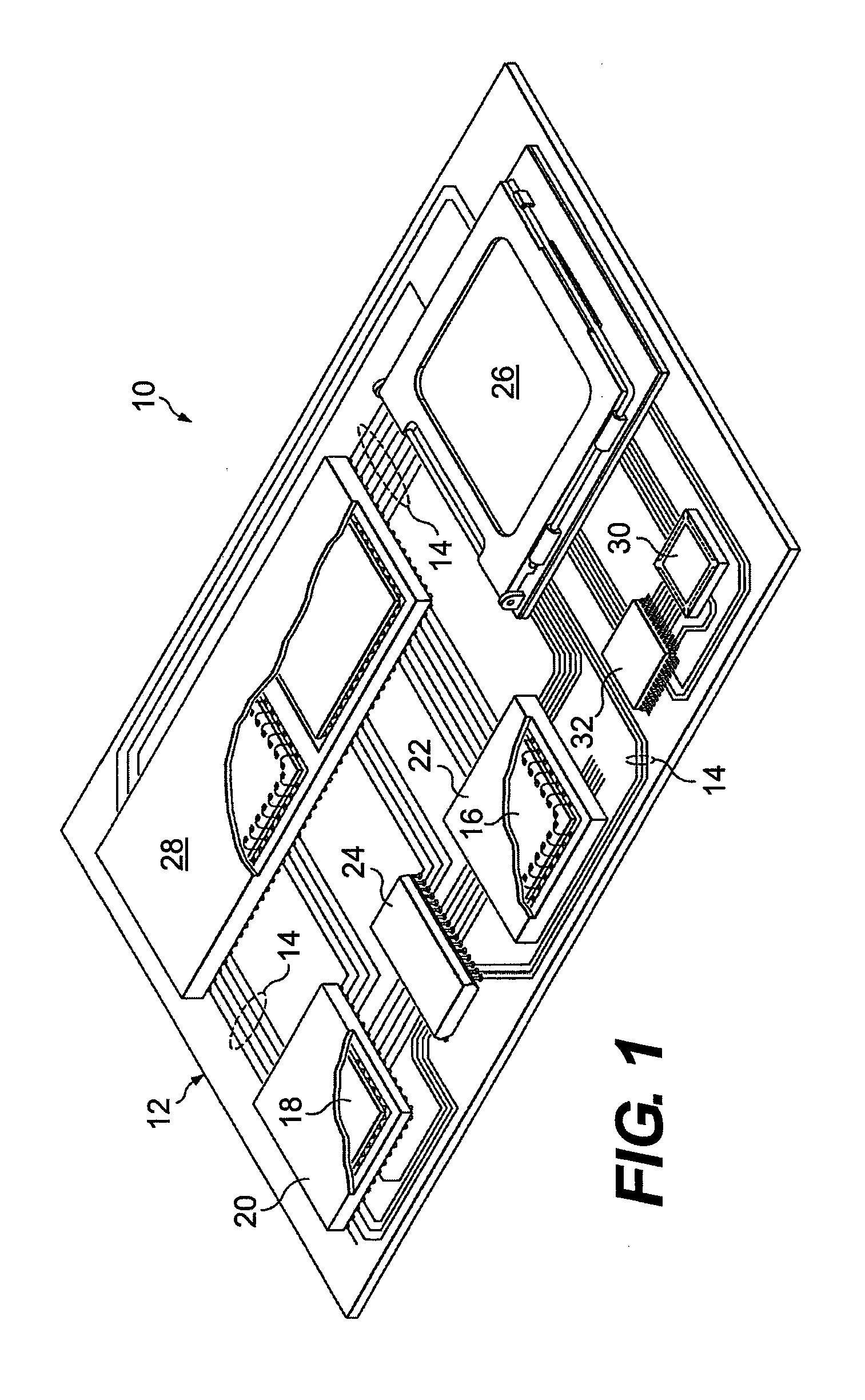
Figure 2 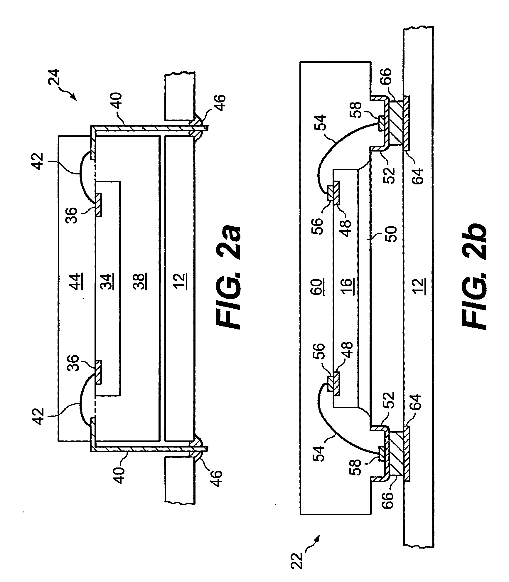
Figure 3
Abstract
Description
CLAIM TO DOMESTIC PRIORITY
[0001] The present nonprovisional application claims the benefit of priority of U.S. Provisional Application Ser. No. 60 / 975,124, filed Sep. 25, 2007, entitled “Encapsulated Bump WLCSP” by Tae Hoan Jang et al.FIELD OF THE INVENTION
[0002] The present invention relates in general to semiconductor devices and, more particularly, to a semiconductor device and method of forming an interconnect structure in a non-active area of the wafer.BACKGROUND OF THE INVENTION
[0003] Semiconductor devices are ubiquitous in modern electronic products. Semiconductor devices vary in the number and density of electrical components. Discrete semiconductor devices generally contain one type of electrical component, e.g., light emitting diode (LED), transistor, resistor, capacitor, inductor, and power metal oxide semiconductor field effect transistor (MOSFET). Integrated semiconductor devices typically contain hundreds to millions of electrical components. Examples of integrated semico...
Examples
Example
DETAILED DESCRIPTION OF THE DRAWINGS
[0018]The present invention is described in one or more embodiments in the following description with reference to the Figures, in which like numerals represent the same or similar elements. While the invention is described in terms of the best mode for achieving the invention's objectives, it will be appreciated by those skilled in the art that it is intended to cover alternatives, modifications, and equivalents as may be included within the spirit and scope of the invention as defined by the appended claims and their equivalents as supported by the following disclosure and drawings.
[0019]Semiconductor devices are generally manufactured using two complex manufacturing processes: front-end manufacturing and back-end manufacturing. Front-end manufacturing involves the formation of a plurality of die on the surface of a semiconductor wafer. Each die on the wafer contains active and passive electrical components which are electrically connected to fo...