
Merged Field Effect Transistor Cells For Switching
a field effect transistor and merged field effect technology, applied in the field of integrated circuit switching devices with merged field effect transistors, can solve the problems of frequency loss, frequency loss, loss due to parasitic capacitances, etc., to reduce the amount of required wiring, reduce resistance, and reduce device size
Patent Information
- Authority / Receiving Office
- US · United States
- Current Assignee / Owner
- Publication Date
- 2009-09-10
- Estimated Expiration
- Not applicable · inactive patent
Smart Images
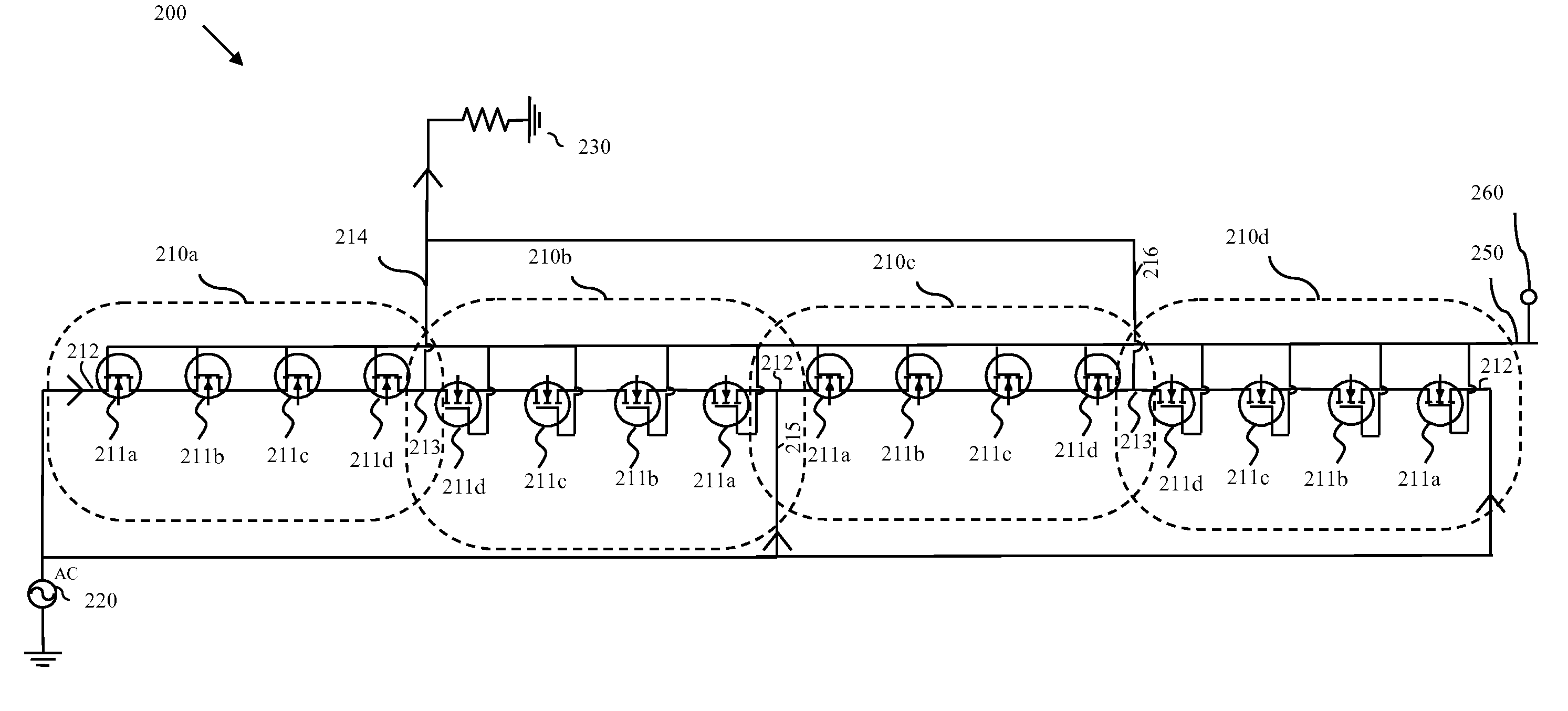
Figure 1 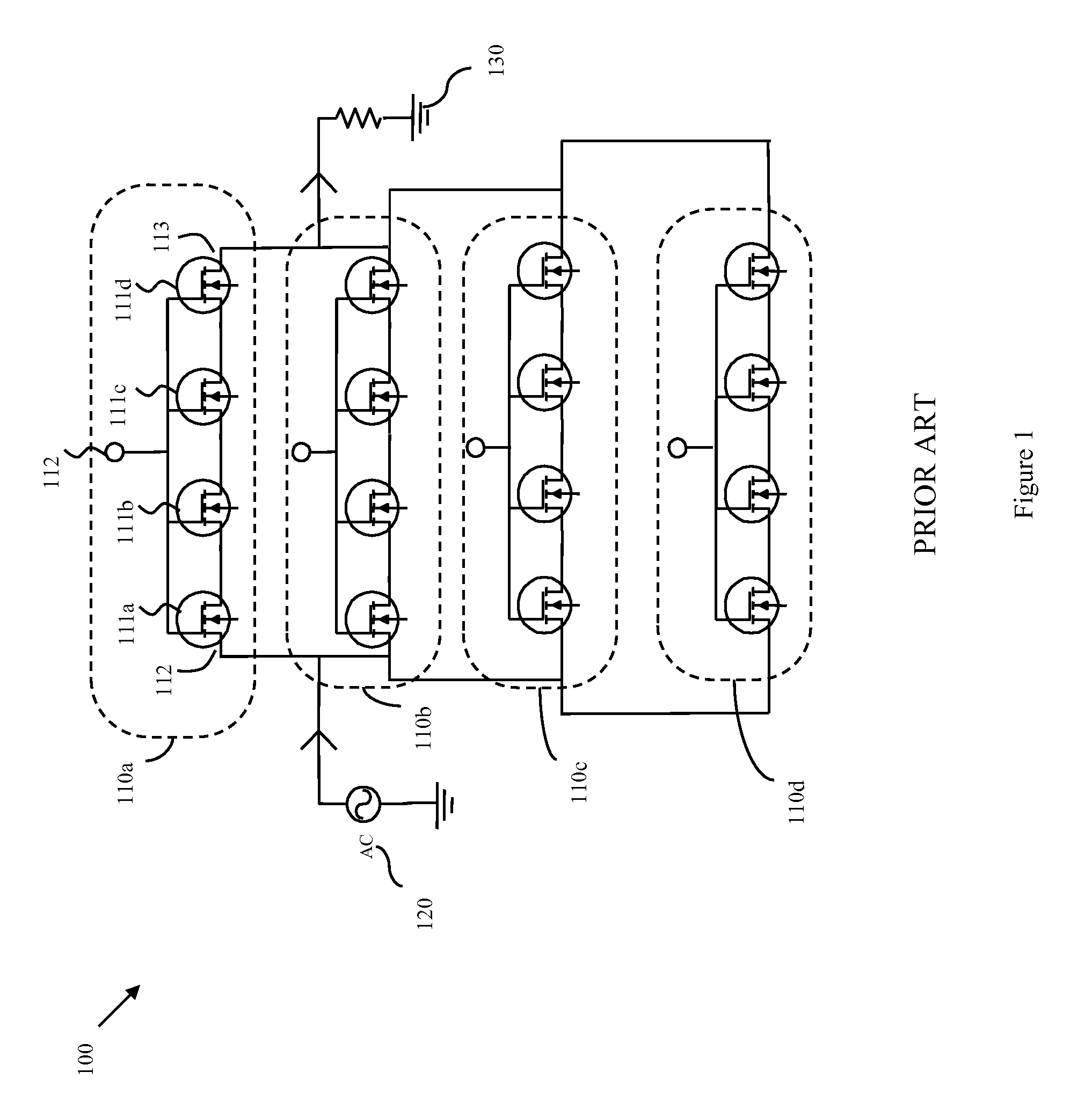
Figure 2 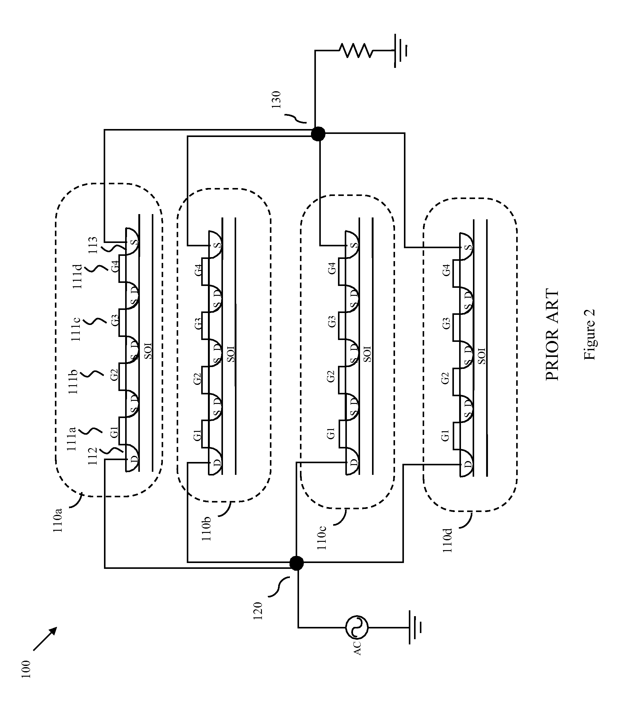
Figure 3
Abstract
Description
BACKGROUND OF THE INVENTION
[0001] The embodiments of the invention generally relate to integrated circuit devices and, more particularly, to an improved integrated circuit switching device with merged field effect transistor (FET) cells for minimized series resistance as well as minimized parasitic capacitance in order to avoid signal frequency losses.
[0002] Numerous integrated circuit applications require switching. Most integrated circuit switching devices (i.e., switches) are implemented with one or more field effect transistors (FETs). A simple FET switch functions by selectively applying a voltage on the FET in order to create a low resistance signal path in the FET channel region between the FET drain and source regions. However, losses in the frequency of this signal as it passes through the channel region can occur due to a number of different factors. For example, parasitic capacitance between the wafer substrate and the drain region, source region and channel region of the F...
Examples
Embodiment Construction
[0024]The embodiments of the invention and the various features and advantageous details thereof are explained more fully with reference to the non-limiting embodiments that are illustrated in the accompanying drawings and detailed in the following description. It should be noted that the features illustrated in the drawings are not necessarily drawn to scale. Descriptions of well-known components and processing techniques are omitted so as to not unnecessarily obscure the embodiments of the invention. The examples used herein are intended merely to facilitate an understanding of ways in which the embodiments of the invention may be practiced and to further enable those of skill in the art to practice the embodiments of the invention. Accordingly, the examples should not be construed as limiting the scope of the embodiments of the invention.
[0025]As mentioned above, numerous integrated circuit applications require switching. Most integrated circuit switching devices (i.e., switches)...