
Semiconductor thin film forming system
Patent Information
- Authority / Receiving Office
- US · United States
- Current Assignee / Owner
- Publication Date
- 2010-01-14
- Estimated Expiration
- Not applicable · inactive patent
Smart Images
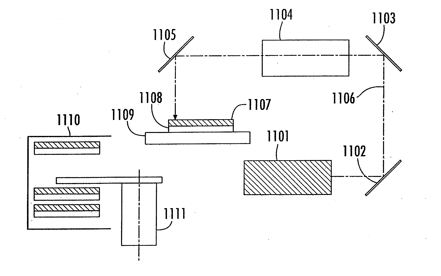
Figure 1 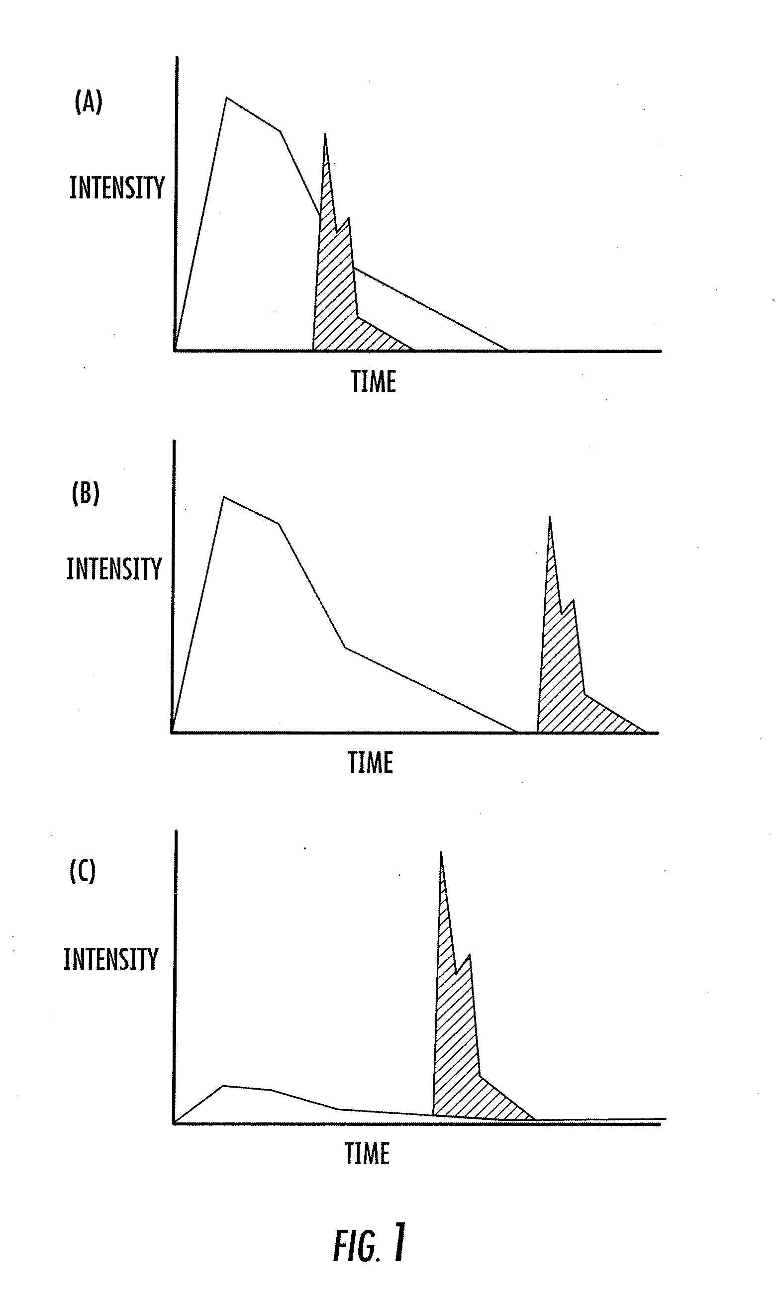
Figure 2 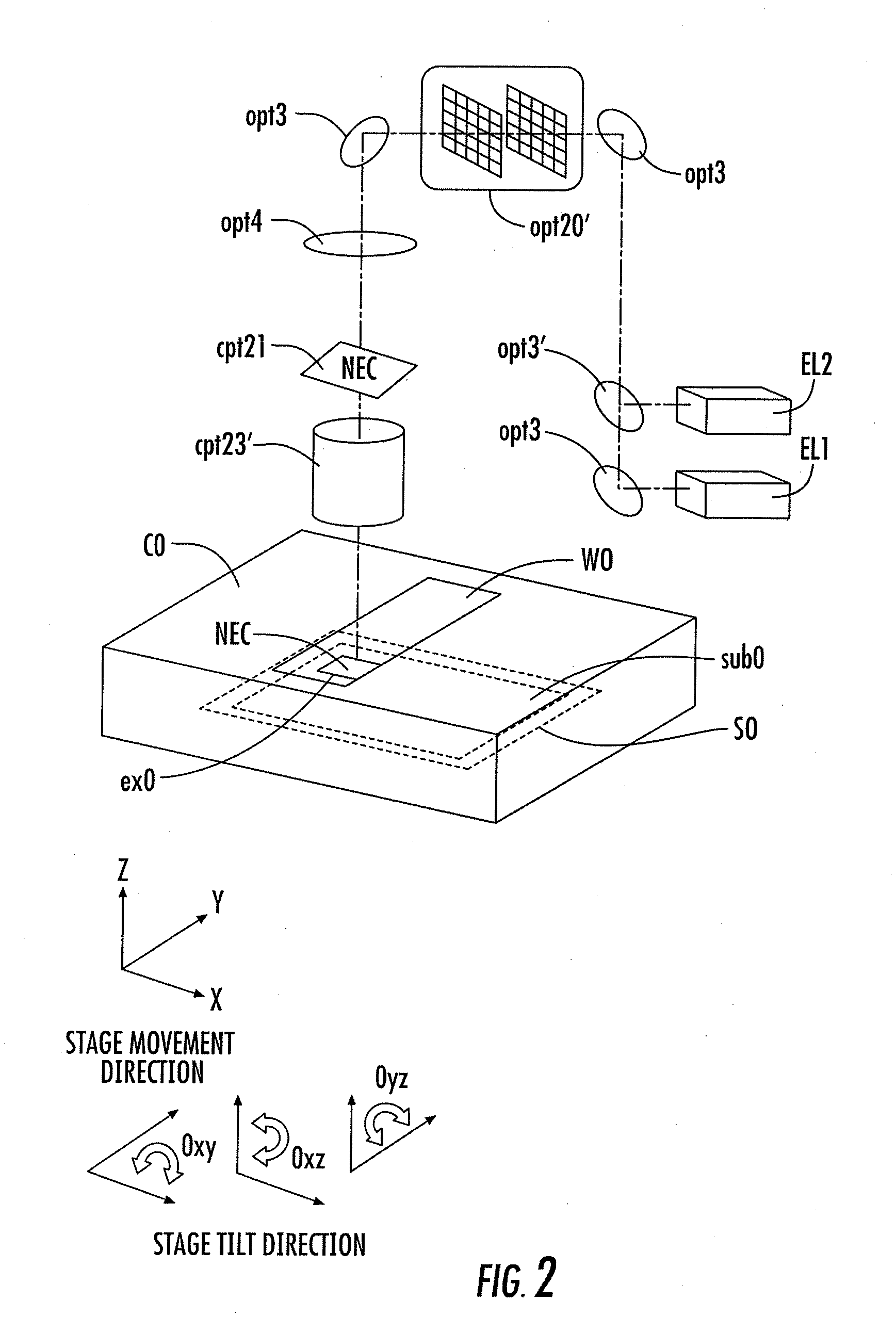
Figure 3
Abstract
Description
CROSS REFERENCE TO RELATED APPLICATIONS
[0001] This application is a divisional of U.S. application Ser. No. 10 / 276,553 filed Jul. 3, 2003, which is a §371 of PCT / JP2001 / 04112, filed May 17, 2001, which claims priority from Japanese Application No. 2000-144363, filed May 17, 2000, the entire contents of each of these applications being incorporated herein by reference in their entirety.BACKGROUND OF THE INVENTION
[0002] 1. Field of the Invention
[0003] This invention relates to a system for the formation of a silicon thin film and a good-quality semiconductor-insulating film interface. Such silicon thin films are used for crystalline silicon thin film transistors, and such semiconductor-insulating film interfaces are employed for field effect transistors. The invention also relates to a semiconductor thin film forming system by the pulsed laser exposure method. In addition, the invention relates to a system for the manufacture of driving elements or driving circuits composed of the semico...
Examples
Embodiment Construction
[0061]The embodiments of the invention will now be illustrated in detail with reference to the drawings.
[0062]FIG. 1 illustrates an example of the embodiment of the present invention. Each of the oscillation start timings is depicted as the abscissa axis while the irradiation energy (i.e., the intensity of pulse irradiation) is depicted as the region bound by the pulse line. FIG. 1(a) shows an example where a second pulse is irradiated with a delay to a first pulse laser. FIG. 1(b) shows an example where a second pulse is irradiated after the completion of the first pulse irradiation. Depending on the constitution of the laser apparatus, the time interval required between the supply of the trigger signal for controlling the oscillation and the actual start of the oscillation. Therefore, it is preferred to calculate and predetermine the “trigger oscillation” time in advance so as to control the irradiation to be started at the simultaneous timing. As compared with the second pulse, t...