
Disc master, disc master manufacturing method, stamper, disc substrate, optical disc, and optical disc manufacturing method
a technology of disc master and manufacturing method, which is applied in the direction of instruments, applications, photomechanical equipment, etc., can solve the problems of degrading separation performance and increasing adhesion between the substrate and the stamper, and achieve the effect of improving separation performance, maintaining signal characteristics, and improving separation performance between the stamper and the disc substra
Patent Information
- Authority / Receiving Office
- US · United States
- Patent Type
- Applications(United States)
- Current Assignee / Owner
- Publication Date
- 2010-02-11
- Estimated Expiration
- Not applicable · inactive patent
Smart Images
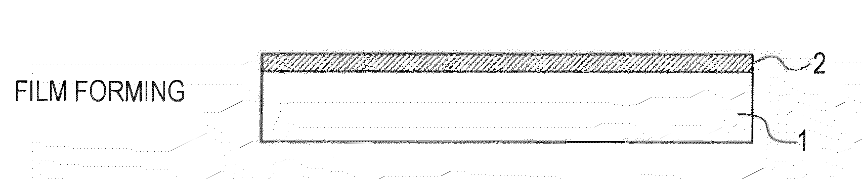
Figure 1 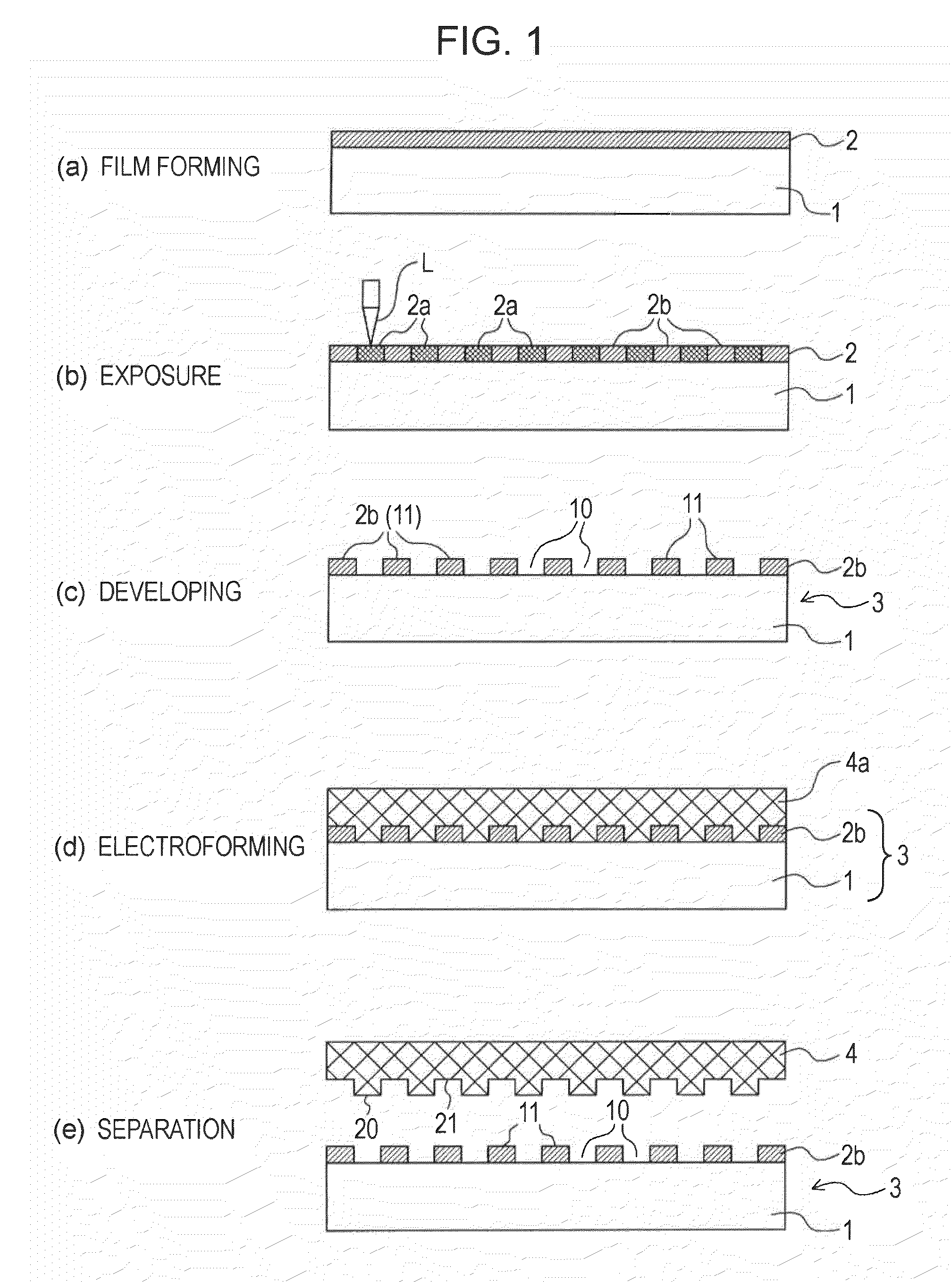
Figure 2 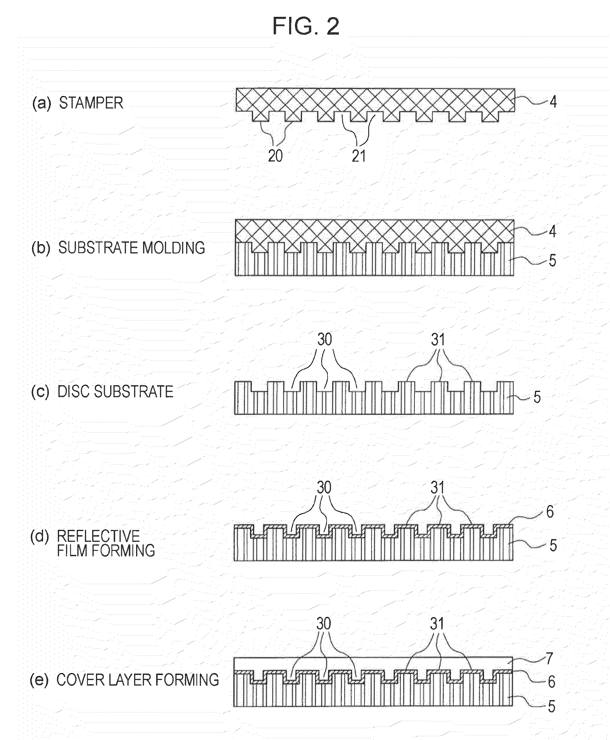
Figure 3
Abstract
Description
TECHNICAL FIELD
[0001] The present invention relates to a disc master, a disc master manufacturing method, a stamper, a disc substrate, an optical disc, and an optical disc manufacturing method.BACKGROUND ARTPatent Document 1: Japanese Unexamined Patent Application Publication No. 2004-152465Patent Document 2: Japanese Unexamined Patent Application Publication No. 2-150325
[0002] Conventionally, in a general optical disc manufacturing method, first, a disc master is manufactured. Then, a stamper is manufactured using the disc master, and disc substrates are mass-produced using the stamper. A layered structure including a reflective film, a cover layer, etc., is formed on the mass-produced disc substrates. Thus, optical discs are completed.
[0003] Here, first, the disc master is formed such that the disc master has a recess-projection pattern for forming a pit / land structure which defines information signal lines, or a recess-projection pattern for forming a groove / land structure which def...
Examples
Embodiment Construction
[0055]Hereinafter, an embodiment of the present invention will be described.
[0056]First, the overall manufacturing process of an optical disc will be described with reference to FIGS. 1 and 2.
[0057]FIG. 1(a) shows the state in which a resist film 2 is formed on a master substrate 1 for forming a disc master.
[0058]The master substrate 1 is, for example, a glass substrate or a silicon wafer substrate.
[0059]In the film forming step, the resist layer 2 made of an inorganic resist material is uniformly formed on the master substrate 1 by sputtering.
[0060]More specifically, a film of inorganic resist is formed using a film-forming device (sputtering device) on the master substrate 1 made of glass or silicon wafer. Thus, a film with a sufficient thickness for forming pits or grooves with a desired height is obtained.
[0061]In the sputtering device, an alloy oxide of a transition metal, for example, is used as a target material. With regard to a film-forming method, DC or RF sputtering is us...