
Semiconductor integrated circuit device
Patent Information
- Authority / Receiving Office
- US · United States
- Current Assignee / Owner
- Publication Date
- 2010-08-12
- Estimated Expiration
- Not applicable · inactive patent
Smart Images
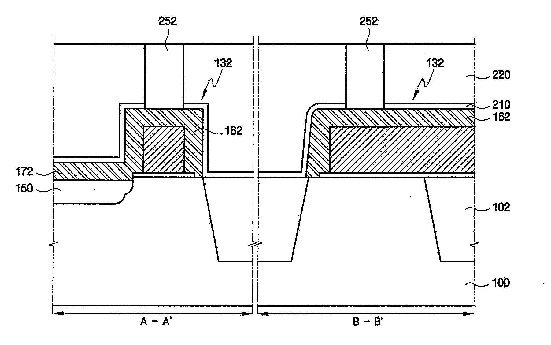
Figure 1 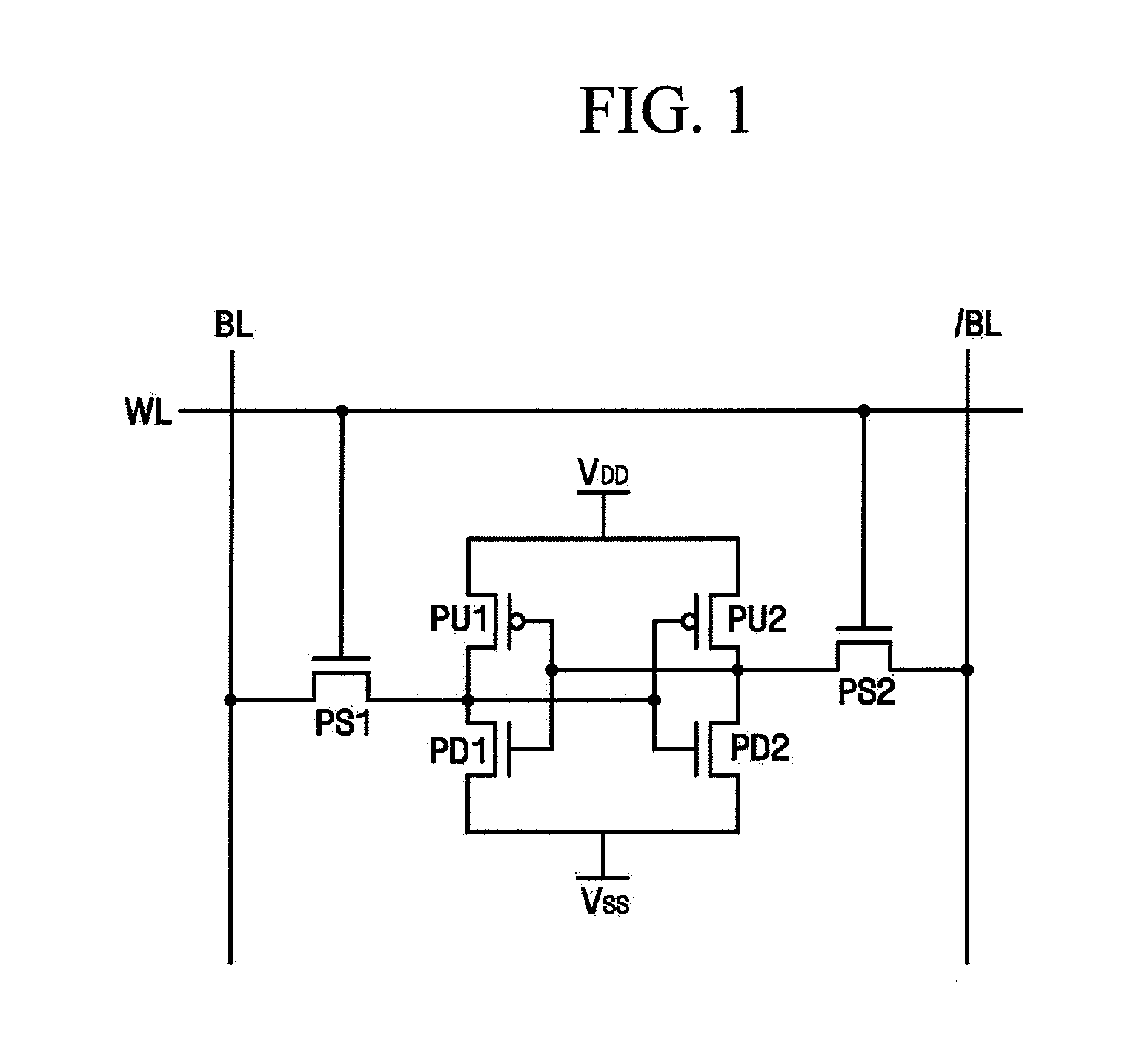
Figure 2 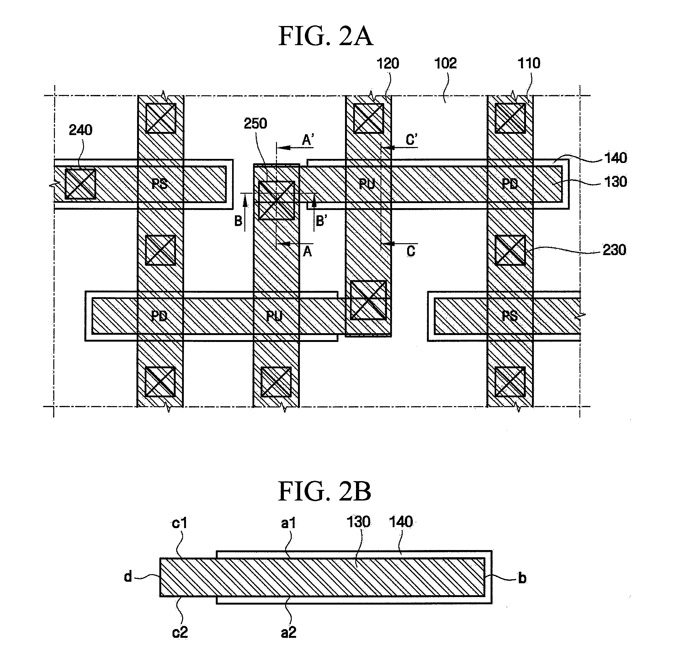
Figure 3
Abstract
Description
[0001] This application claims priority, under 35 U.S.C. §119, of Korean Patent Application No. 10-2009-0010238 filed on Feb. 9, 2009 in the Korean Intellectual Property Office, which is incorporated by reference herein in its entirety.BACKGROUND
[0002] 1. Field of the Invention
[0003] The present invention relates to a semiconductor integrated circuit device, and more particularly, to a semiconductor integrated circuit (IC) memory device with enhanced reliability.
[0004] 2. Description of the Related Art
[0005] Static random access memories (SRAMs) have a smaller memory capacity for a given chip area but a higher operating speed than dynamic random access memories (DRAMs). Accordingly, SRAMs are widely used in cache memories of computers or portable appliances that are required to operate at high speed.
[0006] SRAM cells are divided into thin-layer transistor (TFT) cells and full complementary metal oxide semiconductor (FCMOS) cells. An FCMOS cell includes a plurality of cross-connected pull-...
Examples
Embodiment Construction
[0035]FIG. 1 is a circuit diagram of a static random access memory (SRAM) cell included in a semiconductor integrated circuit (IC) memory device according to exemplary embodiments of the present invention.
[0036]Referring to FIG. 1, the semiconductor integrated circuit device according to the exemplary embodiments includes a six-transistor SRAM cell. The SRAM cell includes a plurality of (e.g., two) pull-up transistors PU1 and PU2 and a plurality of (e.g., two) pull-down transistors PD1 and PD2 which constitute a latch and a plurality of (e.g., two) pass transistors PS1 and PS2 which access the latch.
[0037]Each SRAM memory cell includes first and second pass transistors PS1 and PS2, first and second pull-down transistors PD1 and PD2, and first and second pull-up transistors PU1 and PU2. The first and second pass transistors PS1 and PS2 and the first and second pull-down transistors PD1 and PD2 are n-channel metal oxide semiconductor (NMOS) transistors, and the first and second pull-u...