
Heat assisted magnetic write element
a write element and heat-assist technology, applied in the field of magnetic elements, can solve the problems of high power consumption of the memory making use of such an external magnetic field, risk of accidental switching, and stability of the magnetization of the free layer
Patent Information
- Authority / Receiving Office
- US · United States
- Patent Type
- Applications(United States)
- Current Assignee / Owner
- Publication Date
- 2011-02-24
Smart Images
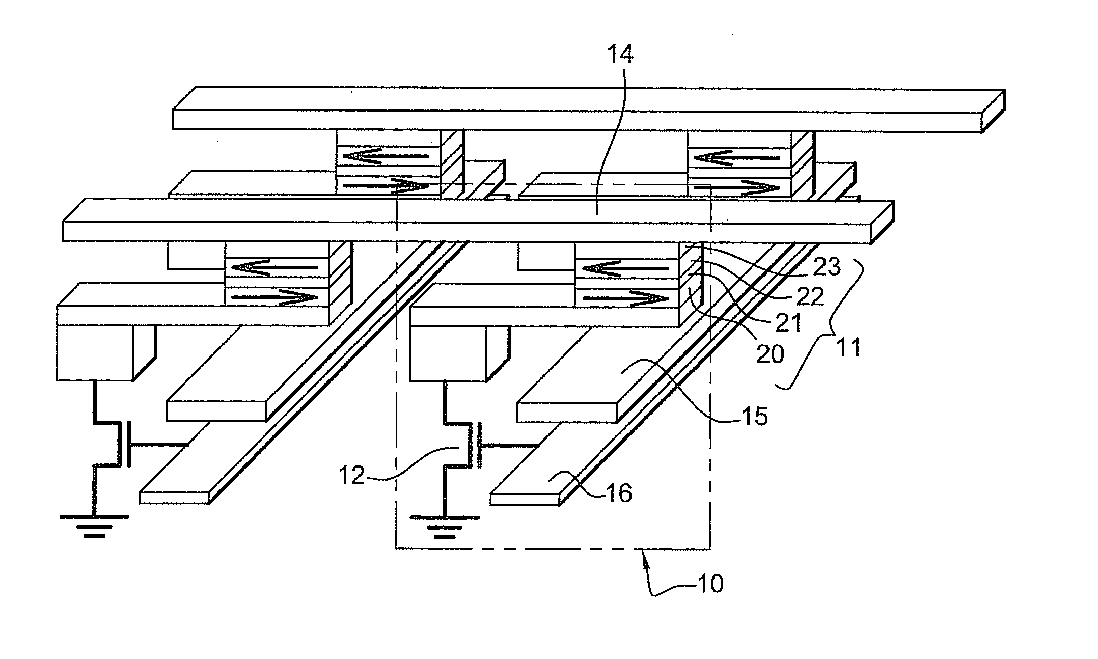
Figure 1 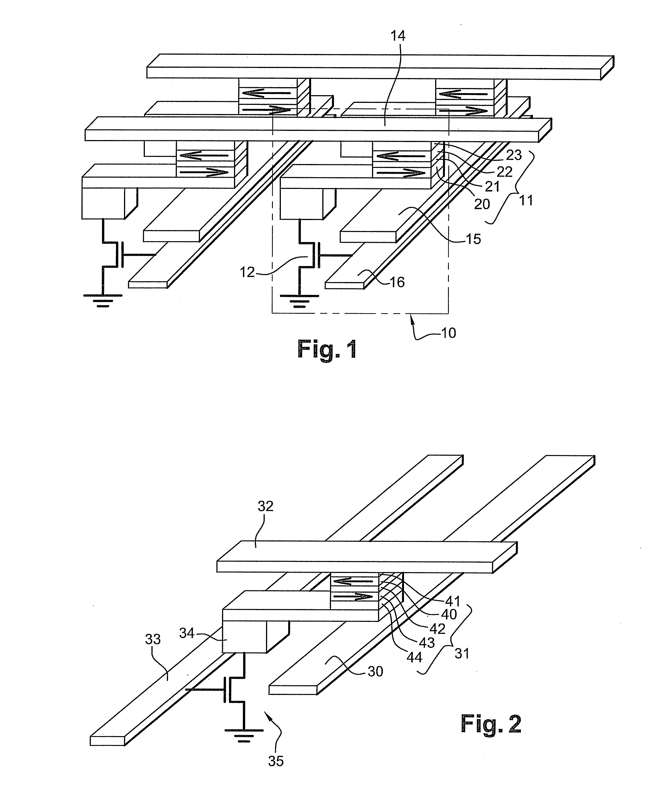
Figure 2 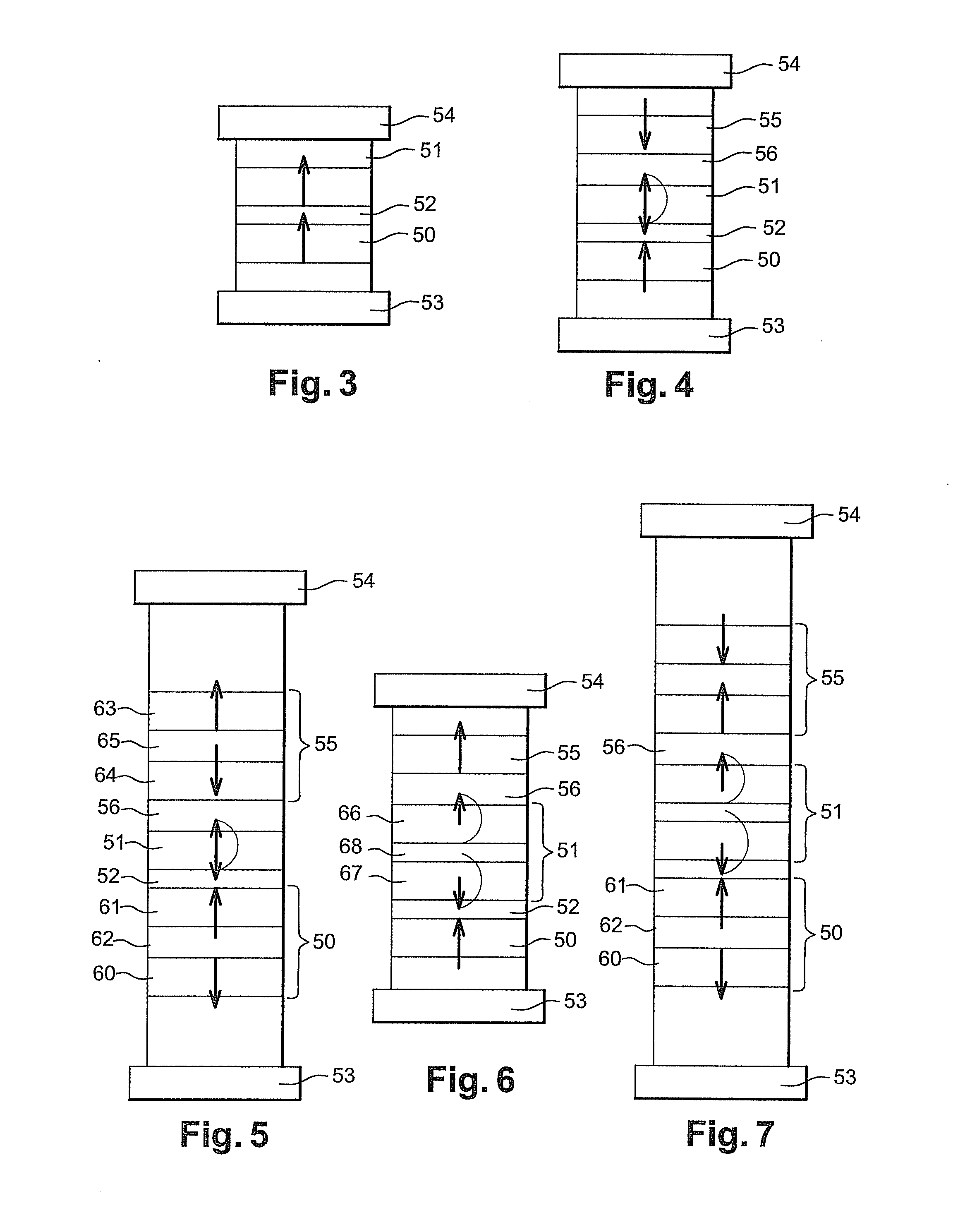
Figure 3
Abstract
Description
TECHNICAL FIELD
[0001] The present invention relates to the field of magnetic elements incorporating a magnetoresistive stack comprising two magnetic layers separated by an insulating tunnel barrier, a confined-current-path layer, a semiconducting layer or a metal layer, and in particular, a magnetic tunnel junction, such as those used in nonvolatile magnetic random access memories, which permit, in a manner known per se, the storage, reading and writing of data in electronic systems. More specifically, it applies to magnetic random access memories, designated conventionally by the acronym MRAM, consisting of a set of memory points each formed by a magnetic tunnel junction, also designated by the acronym MTJ. In a similar manner, the present invention also relates to logic elements having magnetic layers, insofar as they use at least one magnetoresistive stack comprising two magnetic layers separated by an insulating tunnel barrier, a confined-current-path layer, a semiconducting laye...
Examples
Embodiment Construction
[0099]The magnetic element at the core of the memory point or the logic element of the invention is a magnetoresistive element using the giant magnetoresistance or tunnel magnetoresistance effect. The core of this magnetoresistive element basically comprises a sandwich formed of two magnetic layers 50, 51 separated by a non magnetic spacer 52.
[0100]According to the invention, the two magnetic layers have a nonwrite anisotropy perpendicular to the plane of the layers.
[0101]The fixed magnetization layer or reference layer 50 has magnetic properties such that its magnetization remains perpendicular to the plane throughout the temperature range in which the magnetic element operates (in particular during writing and especially during reading and on standby). This operating temperature range may extend from as low as desired to typically +250° C. at the time of writing. There is no lower temperature limit for the operation of a fixed magnetization layer because the out-of-plane anisotrop...