
Method for precisely controlled masked anodization
a technology of masking and anodization, which is applied in the direction of coatings, surface reaction electrolytic coatings, electrolytic coatings, etc., can solve the problem of self-limitation of the anodization process, and achieve the effect of improving and cost-efficien
Patent Information
- Authority / Receiving Office
- US · United States
- Current Assignee / Owner
- Publication Date
- 2012-05-31
- Estimated Expiration
- Not applicable · inactive patent
Smart Images
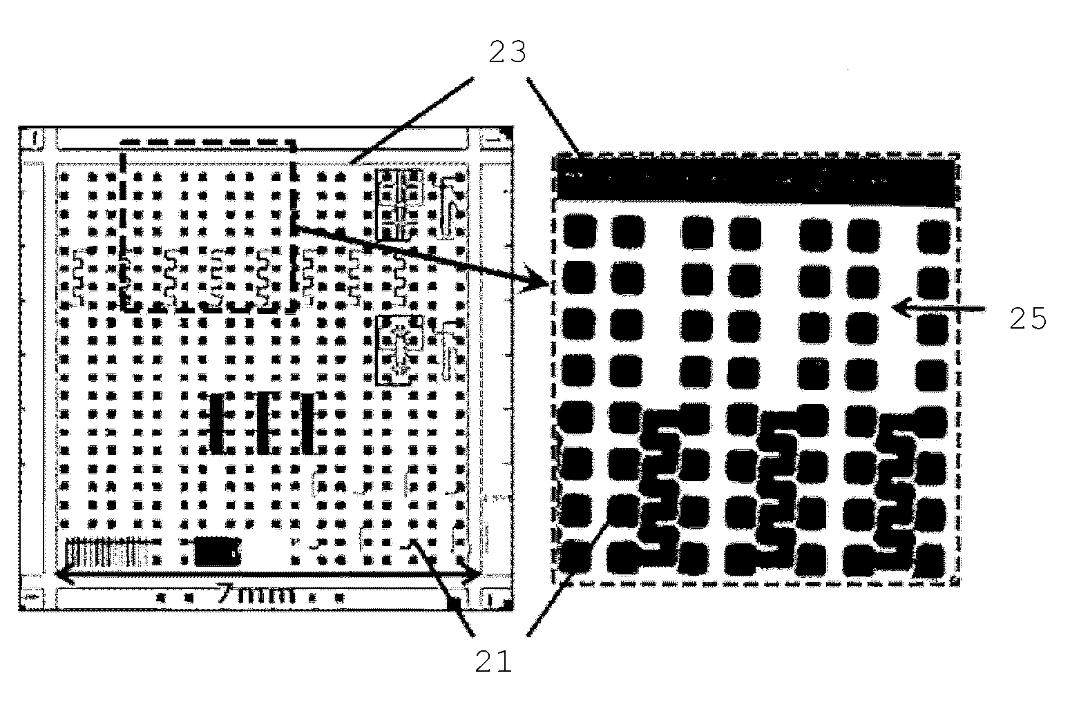
Figure 1 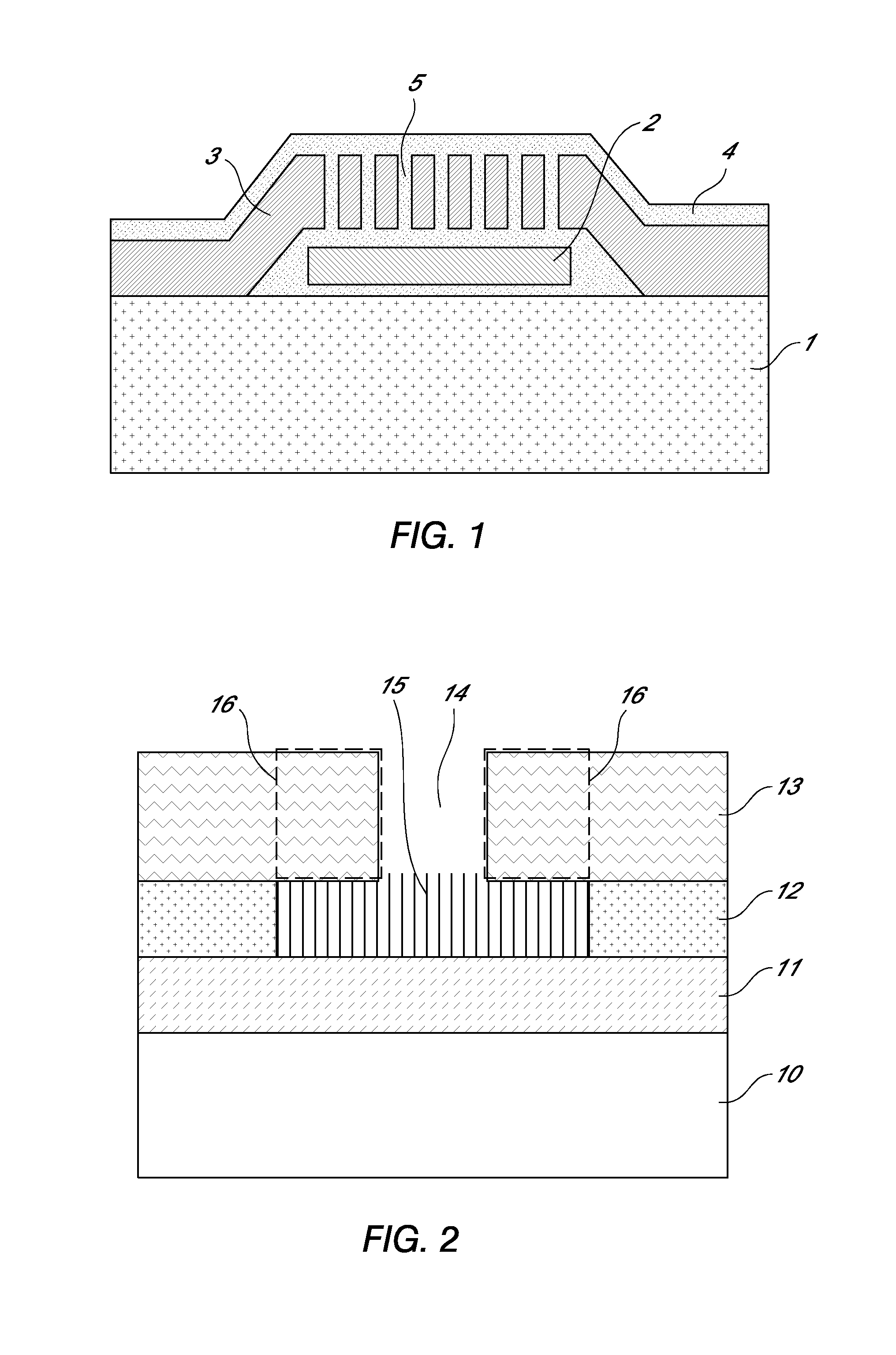
Figure 2 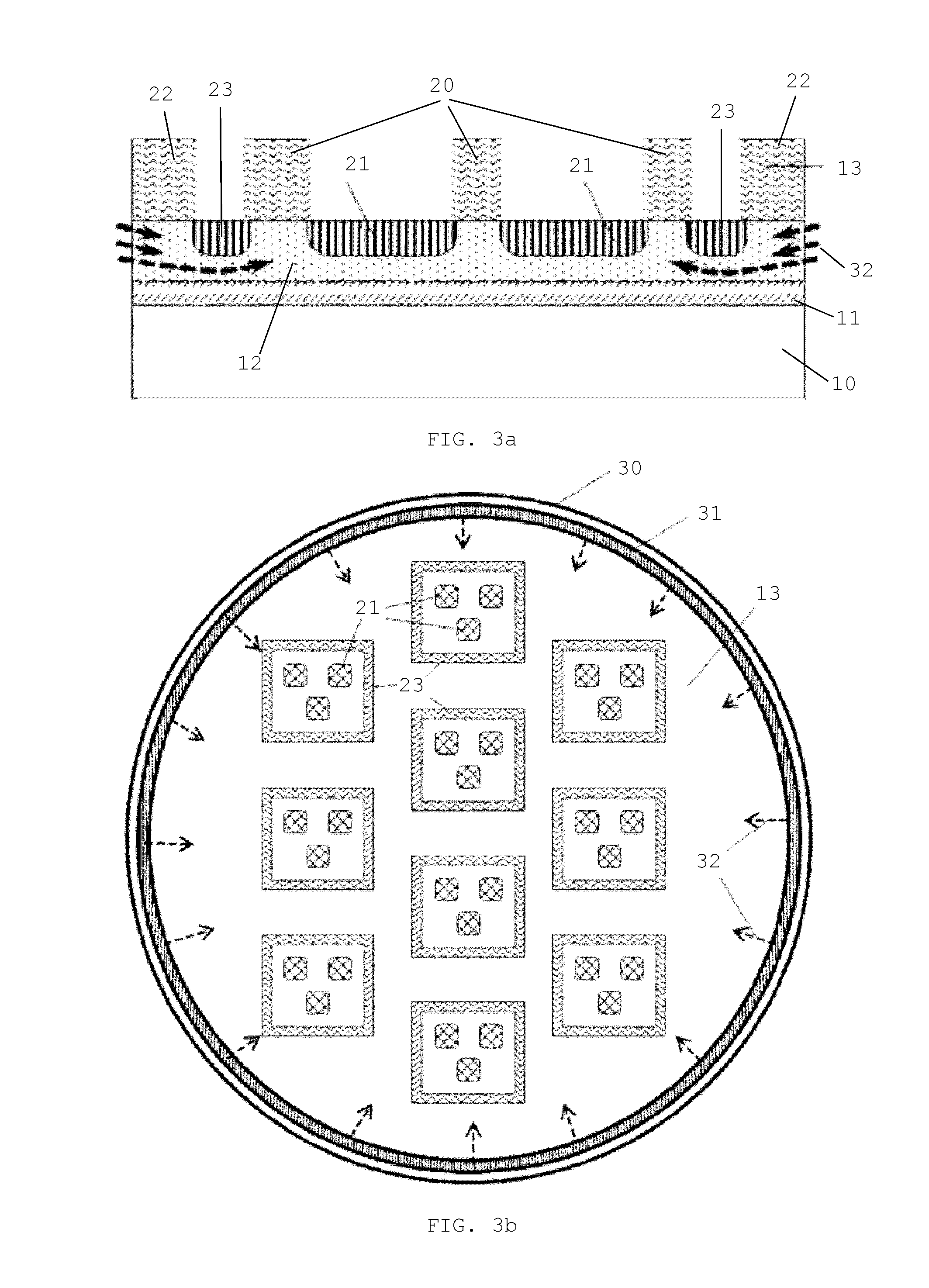
Figure 3
Abstract
Description
CROSS-REFERENCE TO RELATED APPLICATION
[0001] This application claims the benefit under 35 U.S.C. §119(e) of U.S. Provisional Application No. 61 / 418,194, filed Nov. 30, 2010, the disclosure of which is hereby expressly incorporated by reference in its entirety and is hereby expressly made a portion of this application.FIELD OF THE INVENTION
[0002] Methods for precisely controlling a masked anodization process are provided. The preferred embodiments are further related to manufacturing semiconductor devices, especially to methods of encapsulation and to such devices. More specifically they may relate to zero-Level or wafer level packaging of semiconductor devices. More particularly, the preferred embodiments relate to Nano- and / or Micro-Electro-Mechanical Systems (NEMS and / or MEMS) and to processes of encapsulating (or packaging) said systems.BACKGROUND OF THE INVENTION
[0003] Creating patterns of a dielectric or porous material within a conductive thin film by means of masked anodization ...
Examples
examples
[0103]By way of illustration, preferred embodiments not being limited thereto, a number of further particular examples are discussed below, illustrating features and advantages of preferred embodiments.
[0104]In a first particular example, anodization of a 1 μm-thick Al layer (deposited by sputtering on top of a silicon oxide layer on 200 mm Si wafer) has been performed using a photoresist mask not including the border line structure resulting in a large unwanted extension of the anodization region width from 160 μm up to 800 μm as shown in FIG. 2. The anodization process is performed in a Teflon-based chamber housing a sulfuric acid-based electrolyte. The anodization temperature and voltage used here are within the range of 20-30° C. and 10-20V respectively. By performing the same anodization process of an Al layer using a photoresist mask defining a border line 23 (ring) surrounding a plurality of other structures 21 as shown in FIG. 6, the anodization region width has been well co...