
FinFET-Based Memory Testing Using Multiple Read Operations
Patent Information
- Authority / Receiving Office
- US · United States
- Current Assignee / Owner
- Publication Date
- 2018-05-10
Smart Images
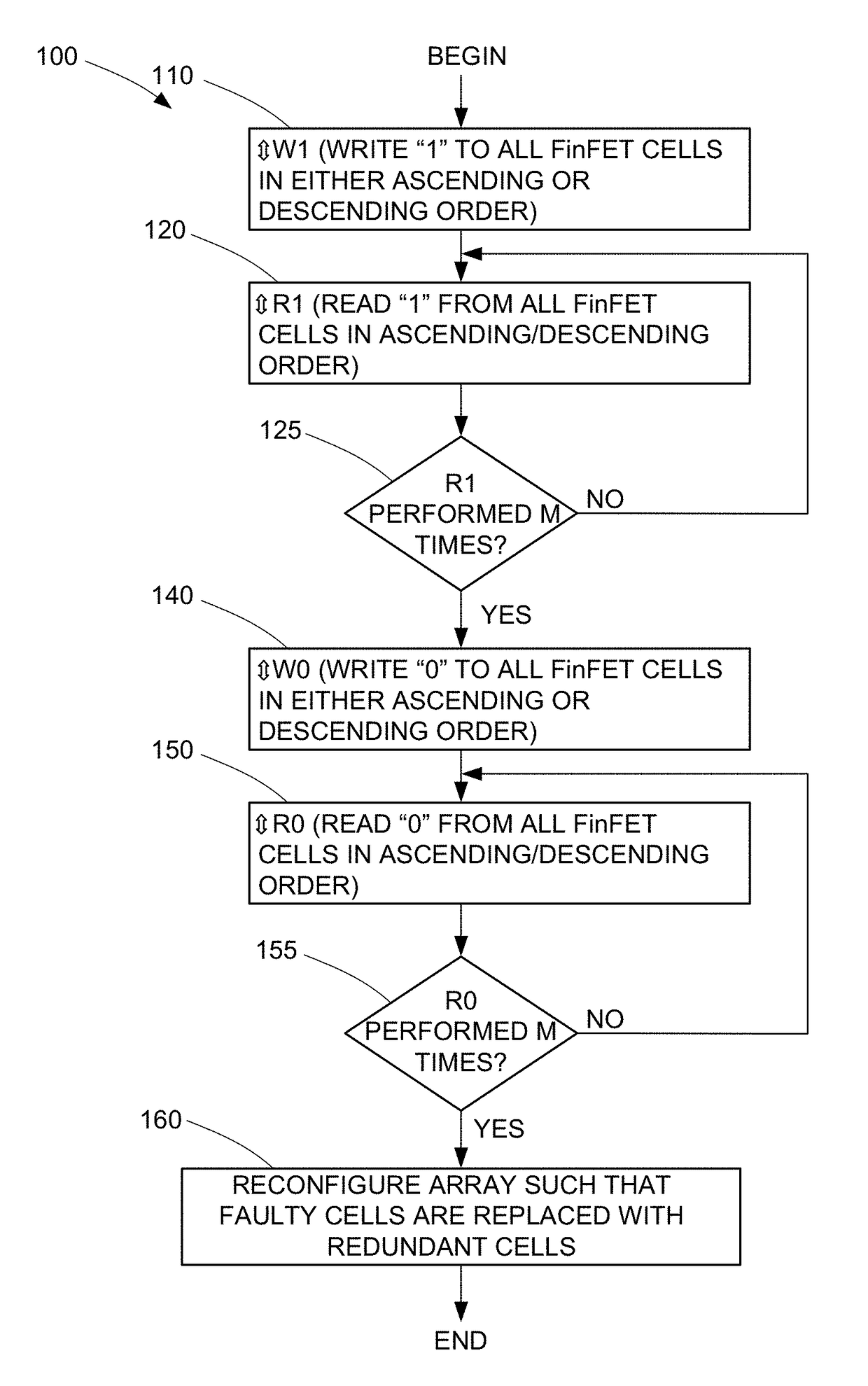
Figure 1 
Figure 2 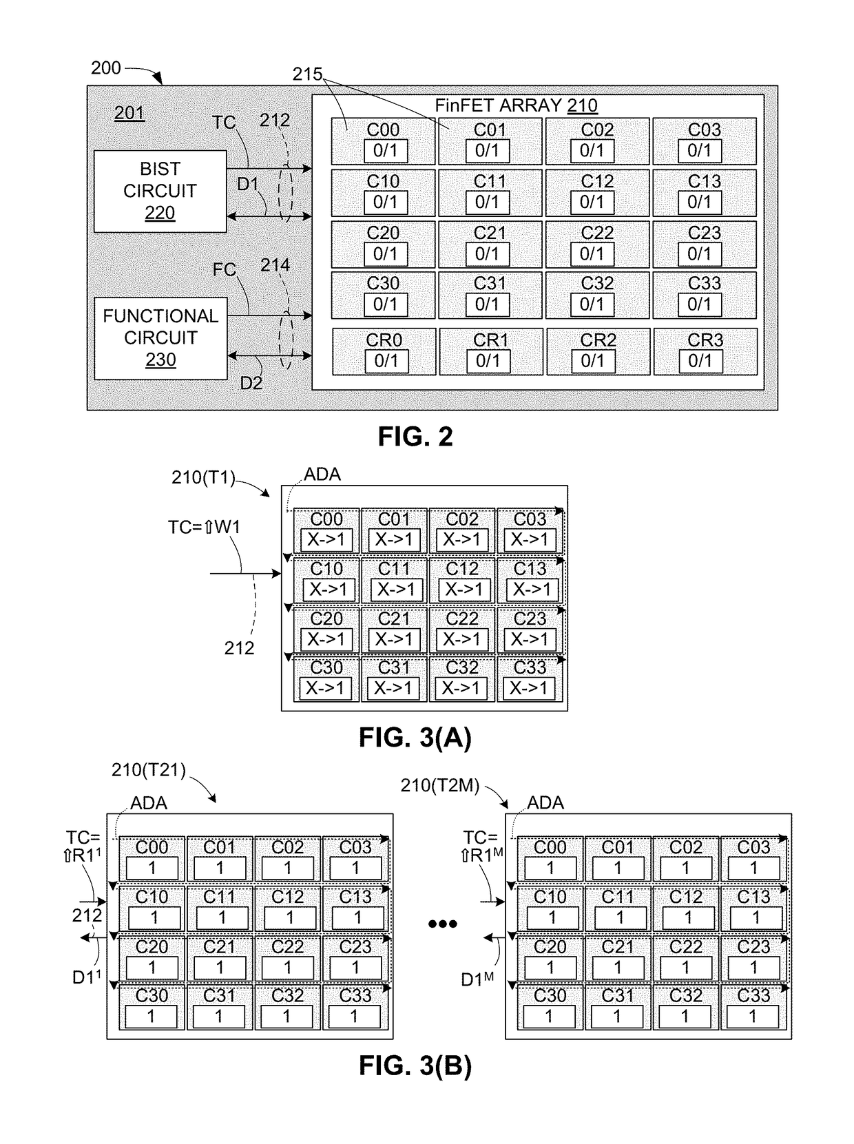
Figure 3
Abstract
Description
RELATED APPLICATION
[0001] This application claims priority from U.S. Provisional Patent Application 62 / 402,598, entitled “BASIC TEST PATTERNS FOR FinFET-BASED MEMORIES”, which was filed on Sep. 30, 2016, and is incorporated by reference herein.FIELD OF THE INVENTION
[0002] This invention relates to testing electronic memories to identify and replace faulty memory cells in embedded memory arrays, and more particularly to modified testing algorithms optimized to identify dynamic faults in embedded FinFET-based memory arrays.BACKGROUND OF THE INVENTION
[0003] Due to the ever increasing demand for cheaper, faster, more complex integrated circuit (IC) devices, IC manufacturers are replacing embedded memories based on standard planar transistor technologies with Fin Field Effect Transistor (FinFET) memories. The phrase “embedded memory” refers herein to on-chip (integrated) electronic memory devices that support a System-on-Chip (SoC) or other IC device's logic core (e.g., one or more micropro...
Examples
Example
DETAILED DESCRIPTION OF THE DRAWINGS
[0029]The present invention relates to an improvement in FinFET memory array testing. The following description is presented to enable one of ordinary skill in the art to make and use the invention as provided in the context of a particular application and its requirements. The terms “coupled” and “connected”, which are utilized herein, are defined as follows. The term “connected” is used to describe a direct connection between two circuit elements, for example, by way of a metal line formed in accordance with normal integrated circuit fabrication techniques. In contrast, the term “coupled” is used to describe either a direct connection or an indirect connection between two circuit elements. For example, two coupled elements may be directly connected by way of a metal line, or indirectly connected by way of an intervening circuit element (e.g., a capacitor, resistor, inductor, or by way of the source / drain terminals of a transistor). Various modif...