
Nitride semiconductor element, nitride semiconductor light emitting element, ultraviolet light emitting element
a technology of semiconductor elements and light emitting elements, applied in the field of nitride semiconductor elements, can solve the problems of reduced resistance and need for further reduction of contact resistance, and achieve the effects of improving the efficiency of carrier high efficiency of the light emitting element 10a, and improving the efficiency of hole injection into the light emitting layer
Patent Information
- Authority / Receiving Office
- US · United States
- Patent Type
- Applications(United States)
- Current Assignee / Owner
- Publication Date
- 2019-05-09
Smart Images
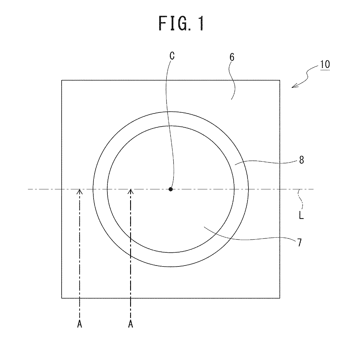
Figure 1 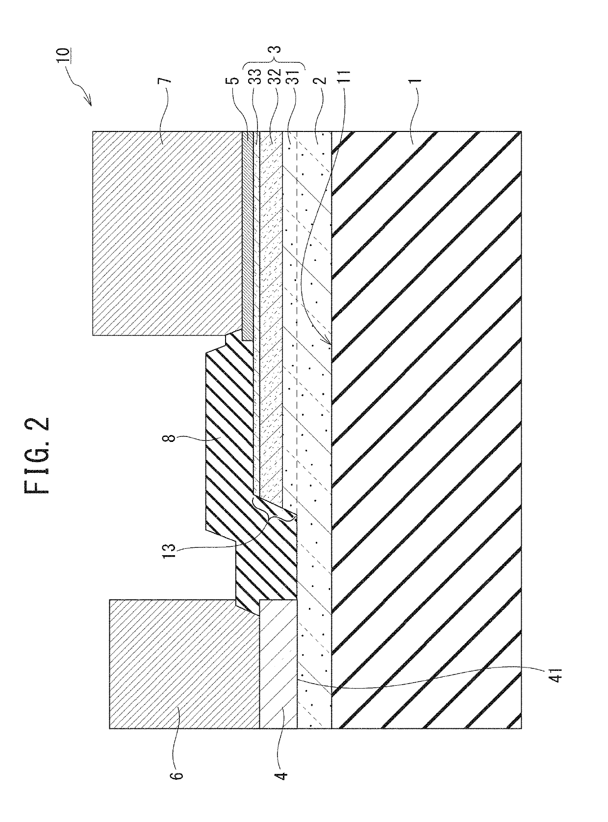
Figure 2 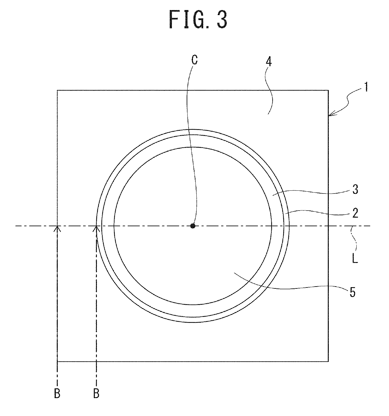
Figure 3
Abstract
Description
BACKGROUND OF THE INVENTIONField of the Invention
[0001] The present invention relates to a nitride semiconductor element.Description of the Related Art
[0002] Nitride semiconductors, such as AlN, GaN, InN, and AlGaN, are attractive materials capable of variously changing the energy band gap by changing the composition ratio of Group III elements (Al, Ga, In).
[0003] In particular, AlGaN has been used for various devices, such as deep UV sensors / light emitting diodes and AlGaN / GaN power devices and transistors. However, AlGaN having a high Al composition is well known as difficult to form an ohmic contact with electrode materials, and thus causing an increase in resistance of AlGaN / electrode interface. Moreover, an electrode contains several metal materials and necessary to be annealed in order to make good contact with AlGaN, and therefore alloys can be formed during the annealing process. When the resistance of the formed alloys is high, the bulk resistance of the electrode increases in...
Examples
embodiments
[0059]Hereinafter, embodiments of the present invention are described but the present invention is not limited to the embodiments described below. The embodiments described below include technically preferable limitations to carry out the present invention but the limitations are not indispensable requirements of the present invention.
first embodiment
[0060]A first embodiment describes an example in which the nitride semiconductor element of the first aspect of the present invention is applied to an ultraviolet light emitting element.
[0061]First, the entire configuration of an ultraviolet light emitting element 10 of this embodiment is described with FIG. 1 to FIG. 3.
[0062]As illustrated in FIG. 1 and FIG. 2, the ultraviolet light emitting element 10 has a substrate 1, an n-type nitride semiconductor layer (first conductivity type first nitride semiconductor layer) 2, a nitride semiconductor body 3, a first electrode layer 4, a second electrode layer 5, a first pad electrode 6, a second pad electrode 7, and an insulation layers 8.
[0063]The n-type nitride semiconductor layer 2 is formed on one surface 11 of the substrate 1. The nitride semiconductor body 3 is a mesa portion formed in a part on the n-type nitride semiconductor layer 2 and has a side surface 13 which is inclined. As illustrated in FIG. 2, the nitride semiconductor b...
second embodiment
[0105]A second embodiment describes an example in which the nitride semiconductor light emitting element of the second aspect of the present invention is applied to an ultraviolet light emitting element. The conductivity type of a first Group III nitride semiconductor layer is set to an n-type and the conductivity type of a second Group III nitride semiconductor layer is set to a p-type.
[0106]First, the entire configuration of an ultraviolet light emitting element 10A of this embodiment is described with FIG. 7 and FIG. 8.
[0107]As illustrated in FIG. 7, the ultraviolet light emitting element 10A has a substrate 1, an n-type Group III nitride semiconductor layer (first Group III nitride semiconductor layer) 20, a nitride semiconductor body 30, a first electrode layer 4, a second electrode layer 5, a first pad electrode 6, a second pad electrode 7, and an insulation layers 8. The n-type Group III nitride semiconductor layer 20 is formed on the substrate 1. The nitride semiconductor bo...