
Ionizing sputtering method
a technology of ionizing sputtering and sputtering chamber, which is applied in the direction of vacuum evaporation coating, coating, electric discharge tube, etc., can solve the problems of difficult formation of a film with a high bottom coverage, critical flaws in the device characteristics, and thin barrier film at the bottom of the hole, so as to achieve less generation of particulates, reduce the formation of particulates, and greatly improve the bottom coverage
Patent Information
- Authority / Receiving Office
- US · United States
- Current Assignee / Owner
- Publication Date
- 2002-09-03
- Estimated Expiration
- Not applicable · inactive patent
Smart Images
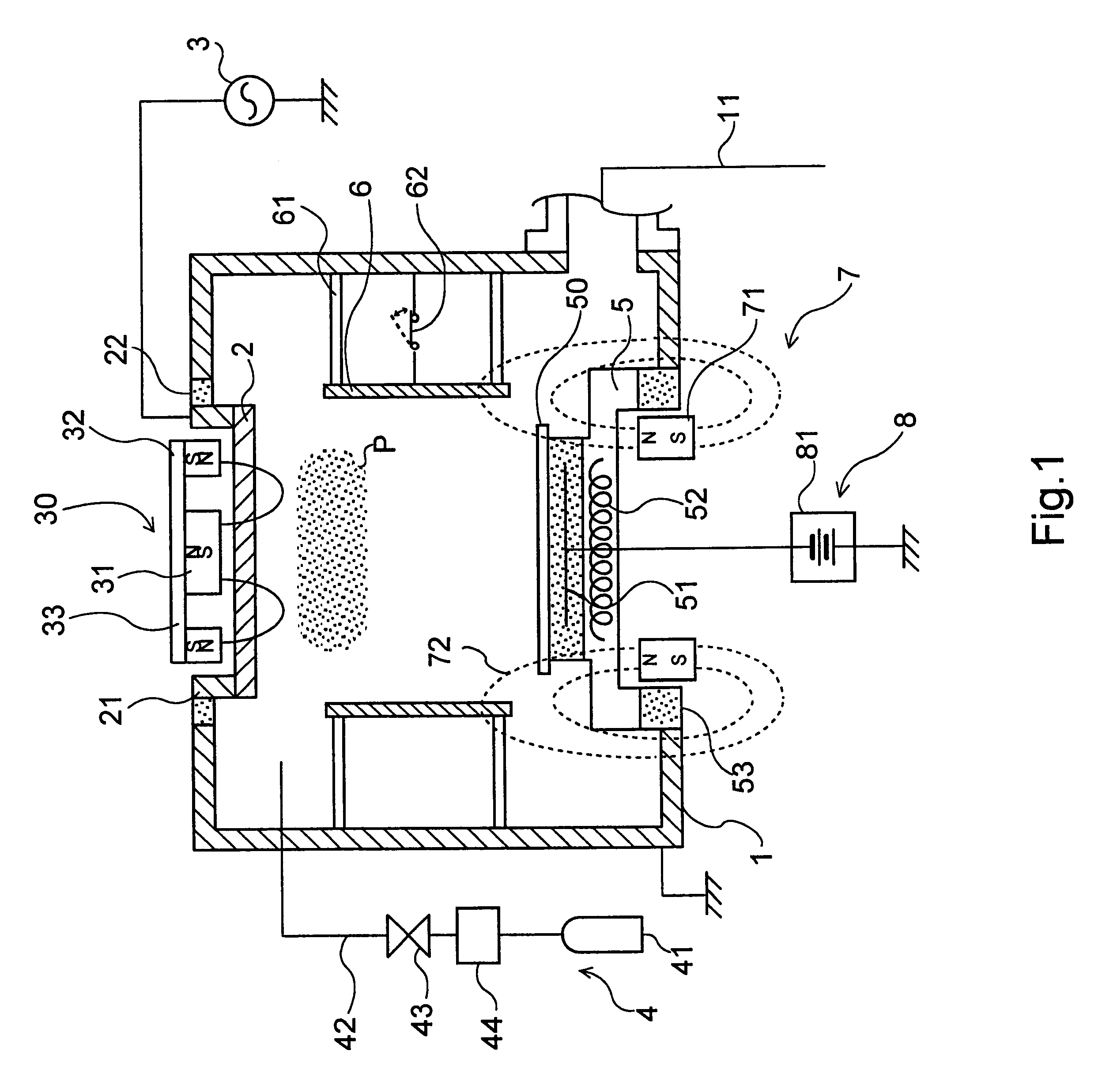
Figure 1 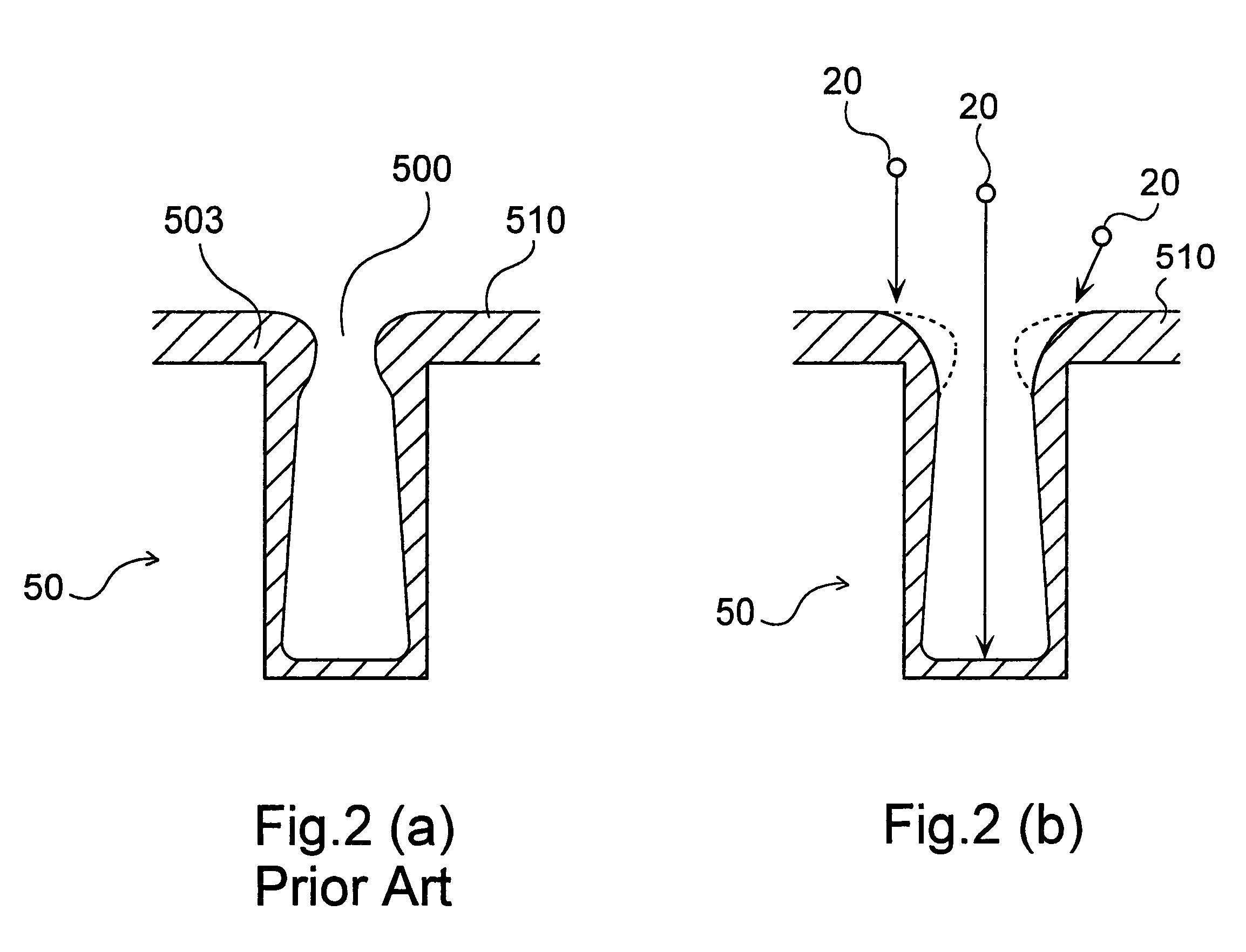
Figure 2 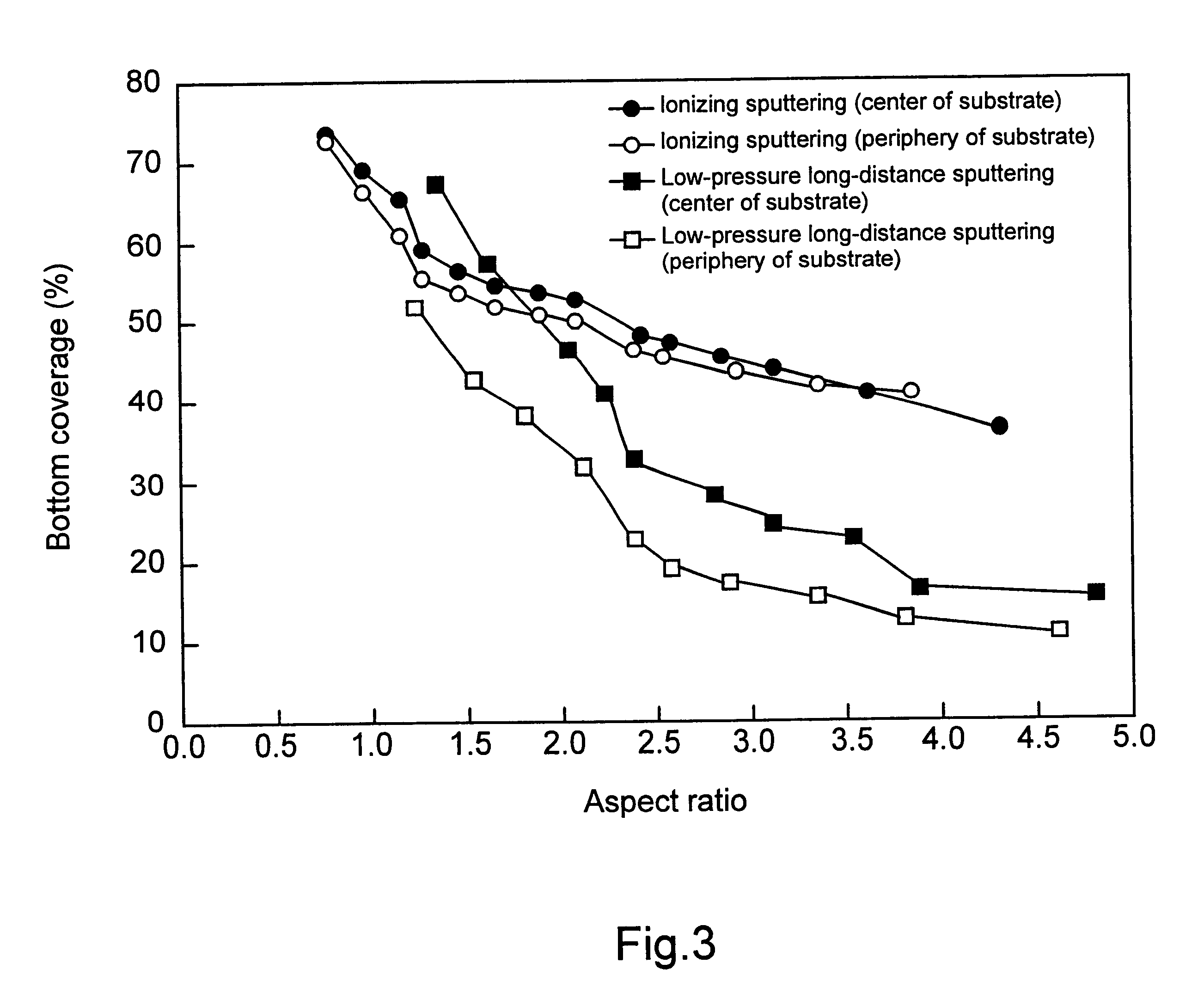
Figure 3
Abstract
Description
This application claims priority under 35 U.S.C. .sctn..sctn. 119 and / or 365 to Japanese Application No. 9-155981 filed in Japan on May 28, 1997; the entire content of which is hereby incorporated by reference.1. Field of Industrial UtilizationThe present invention relates to a sputtering method used in the fabrication of various types of semiconductor devices. More particularly, it relates to an ionizing sputtering method utilized in the formation of films by the ionization of sputter particles.2. Description of Related ArtWith semiconductor devices, such as various types of memory and logic devices, a sputtering process is used in the formation of various wiring films, and in the production of barrier films that prevent the interdiffusion of different layers, and sputter devices are commonly used for this purpose. There has recently been a great need for such sputtering devices to allow the inner surfaces of holes formed in a substrate to be coated with a good degree of coverage.A...
Examples
example 2
Sputtering can be carried out under the following conditions as a practical example (hereinafter referred to as the second practical example) of producing a titanium nitride thin film for use as a barrier film.
Sputtering power source 3: 13.56 MHz, 8 kW output
Material of target 2: titanium
Type of process gas: mixed gas of argon and nitrogen
Flux of process gas: argon 25 cc / min; nitrogen 75 cc / min
Pressure during film deposition: 45 mTorr
Substrate-biasing voltage: -600 V
Temperature of substrate holder 5 during film deposition:
200.degree. C.
Deposition rate: 200 angstroms / min
FIG. 3 is a graph of the results obtained by depositing a film under the conditions of the abovementioned first practical example. The graph shows the relationship of bottom coverage to the aspect ratio of the hole. For the sake of comparison, data are also shown for a conventional, low-pressure, long-distance sputter device. The data for this low-pressure, long-distance sputtering were obtained under conditions compr...