
Electro-optical device, method of manufacturing the same, and electronic apparatus
a manufacturing method and electronic technology, applied in non-linear optics, identification means, instruments, etc., can solve the problems of deterioration of breakdown voltage performance, subject of electronic optical devices according to the related art technology, etc., to simplify manufacturing processes and avoid damage
Patent Information
- Authority / Receiving Office
- US · United States
- Patent Type
- Patents(United States)
- Current Assignee / Owner
- Publication Date
- 2008-06-17
Smart Images
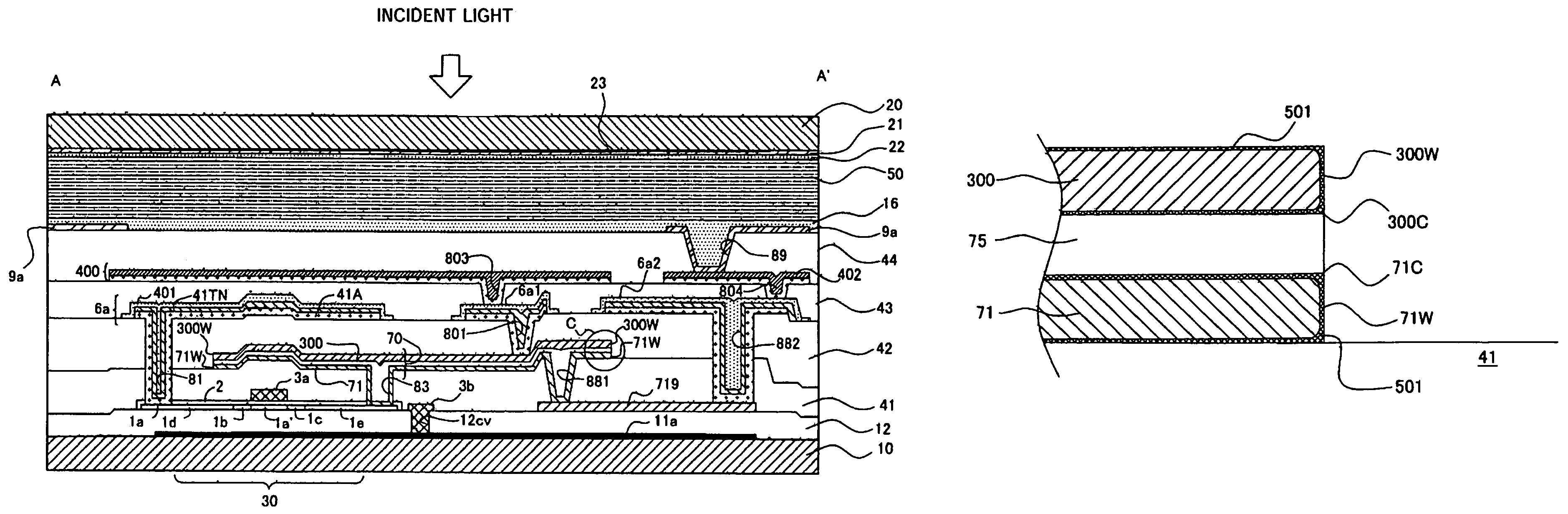
Figure 1 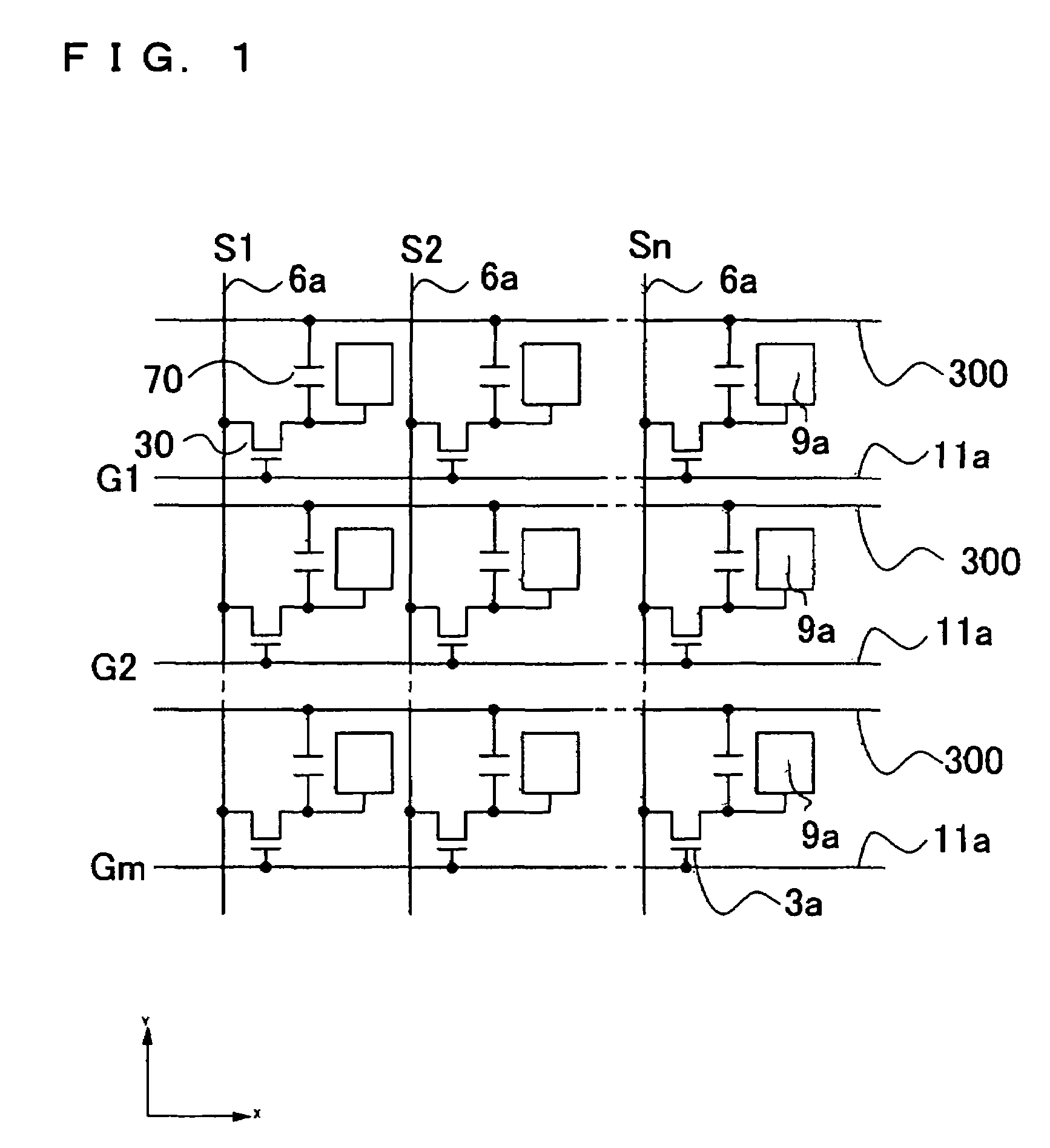
Figure 2 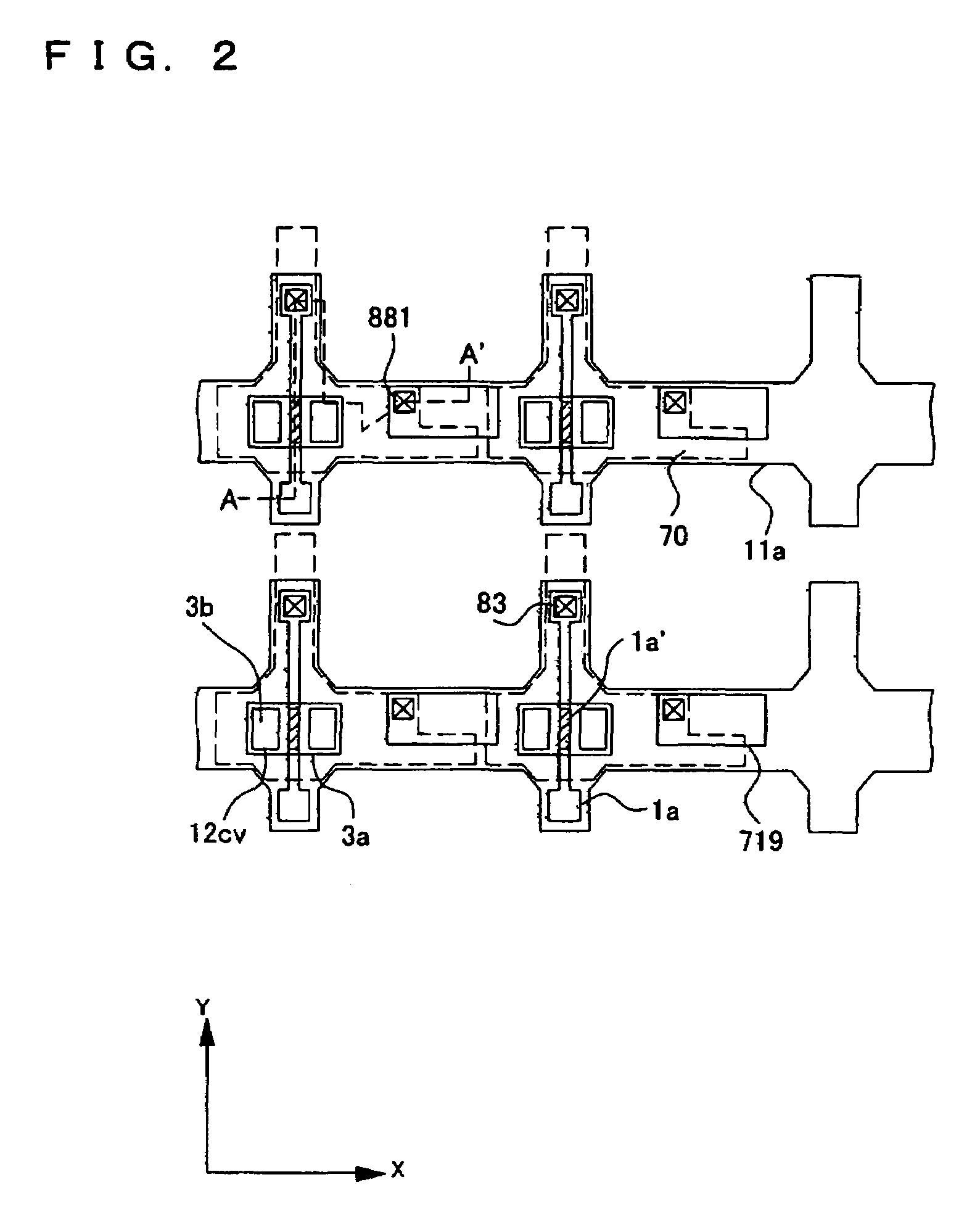
Figure 3
Abstract
Description
BACKGROUND OF THE INVENTION
[0001] 1. Field of Invention
[0002] The present invention relates to electro-optical devices such as an active-matrix-driving liquid crystal device, an electrophoresis device such as electronic paper, an electro-luminescent (EL) display device, and a device including an electron emission element such as a field emission display and a surface-conduction electron-emitter display, and to a method for manufacturing the same. Also, the present invention relates to electronic apparatus including the electro-optical device.
[0003] 2. Description of Related Art
[0004] The related art includes electro-optical devices capable of active-matrix-driving. The related art electro-optical devices include pixel electrodes arranged on a substrate in a matrix, thin film transistors (TFT) connected to each of the pixel electrodes, and data lines and scanning lines connected to the TFTs and provided in parallel in column and row directions.
[0005] The electro-optical device of the rela...
Examples
Embodiment Construction
[0095]Exemplary embodiments of the present invention will now be described with reference to the drawings. According to the exemplary embodiment, an electro-optical device according to the present invention is applied to a liquid crystal device.
[0096]The structure of a pixel portion of an electro-optical device according to an exemplary embodiment of the present invention will now be described with reference to FIGS. 1 to 4. Here, FIG. 1 is a schematic that shows an equivalent circuit of various elements, wiring lines, etc. in a plurality of pixels formed in a matrix that constitutes an image display region of the electro-optical device. FIGS. 2 and 3 are schematics that show plan views of a plurality of pixel groups adjacent to each other on a TFT array substrate on which data lines, scanning lines, and pixel electrodes are formed. Also, FIGS. 2 and 3 respectively illustrate a lower portion (FIG. 2) and an upper portion (FIG. 3) in a laminated structure to be described later. FIG. ...