
Run to run control process for controlling critical dimensions
a control process and critical dimension technology, applied in semiconductor/solid-state device testing/measurement, measurement devices, instruments, etc., can solve problems such as speed performance and power consumption of circuits, loss of linewidth control including the entire loss, contamination with airborne particles and air bubbles, etc., to achieve substantially improved control of critical dimension uniformity, improve manufacturability and control
Patent Information
- Authority / Receiving Office
- US · United States
- Patent Type
- Patents(United States)
- Current Assignee / Owner
- Publication Date
- 2007-03-13
- Estimated Expiration
- Not applicable · inactive patent
Smart Images
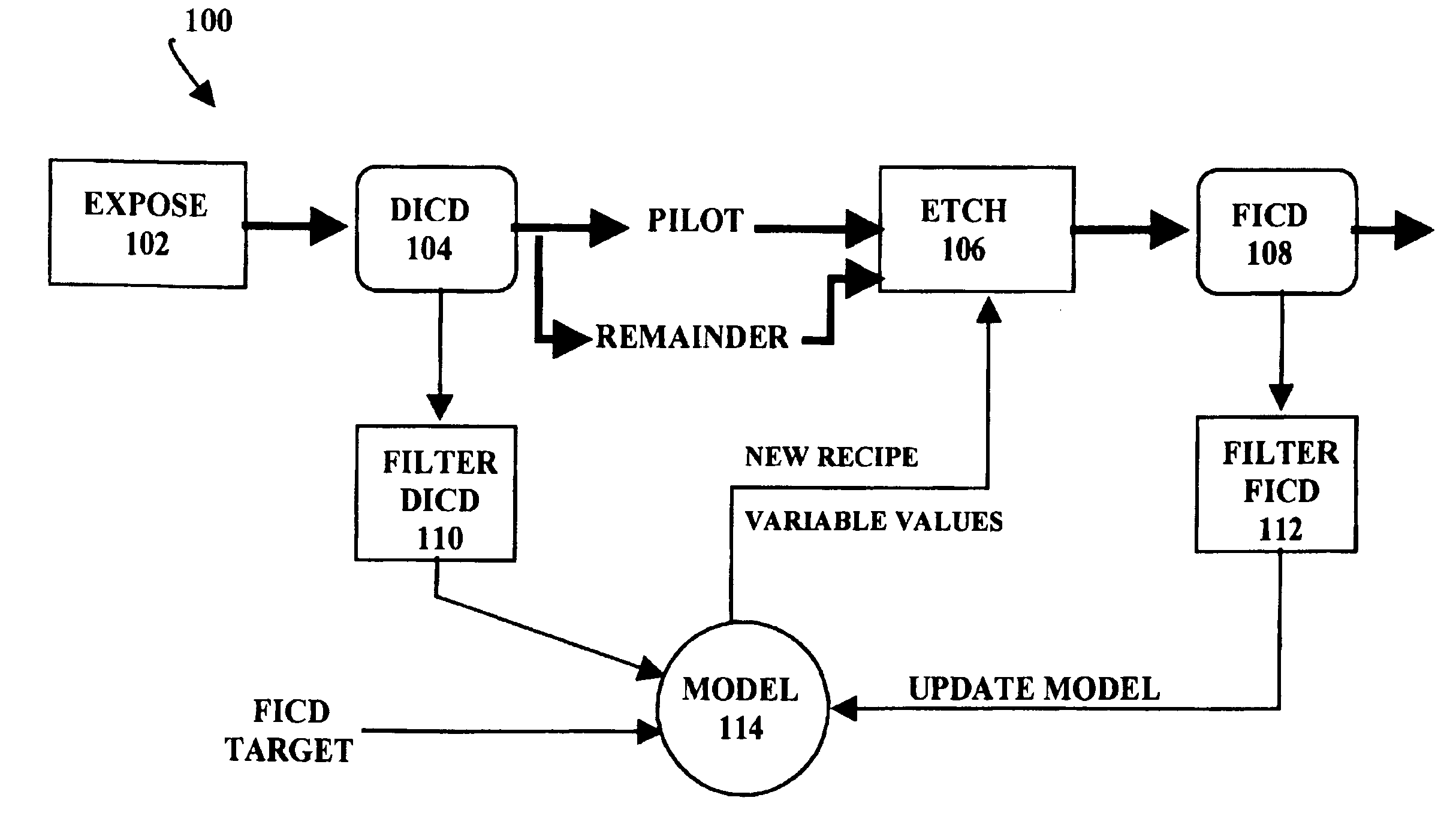
Figure 1 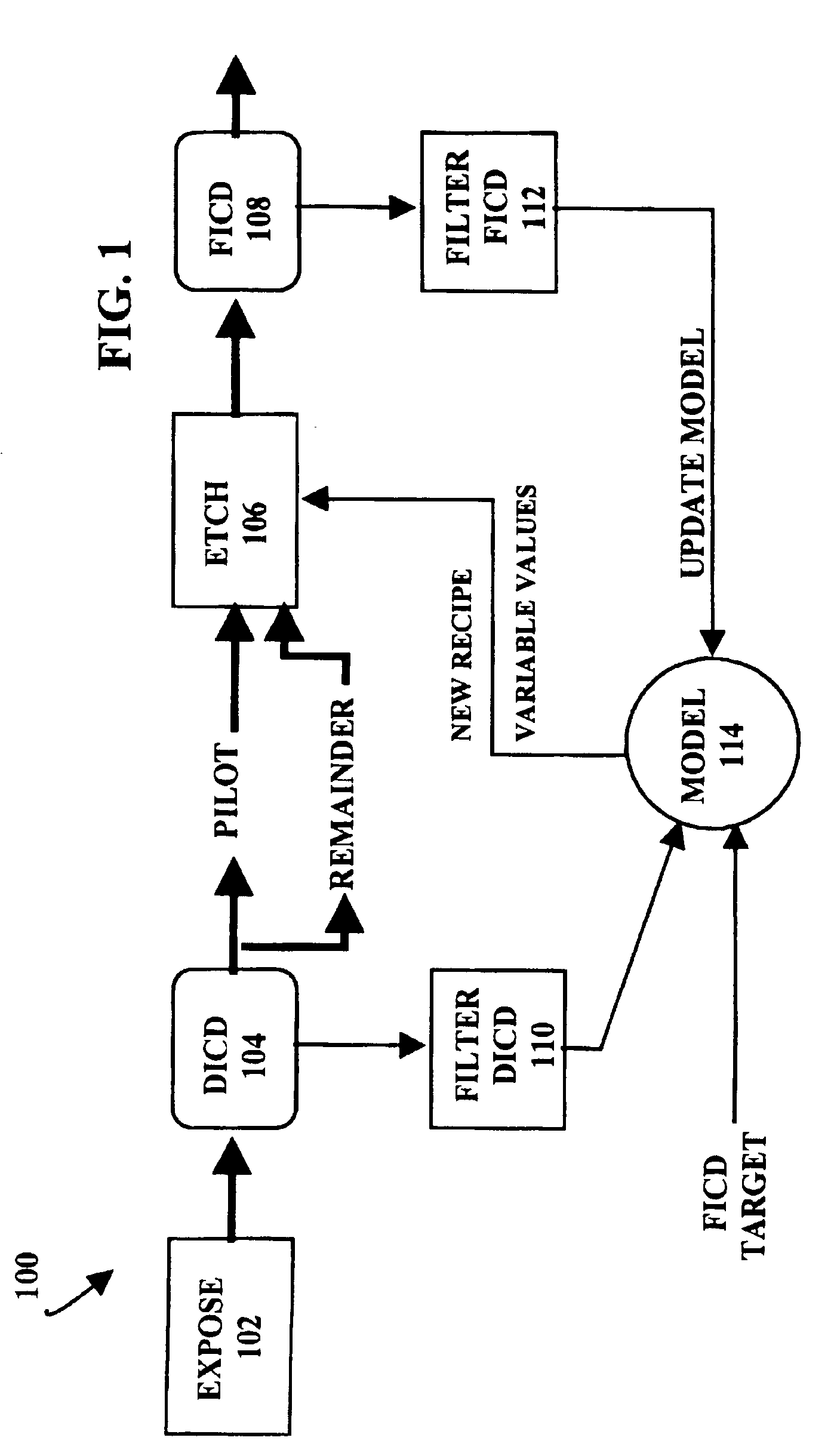
Figure 2 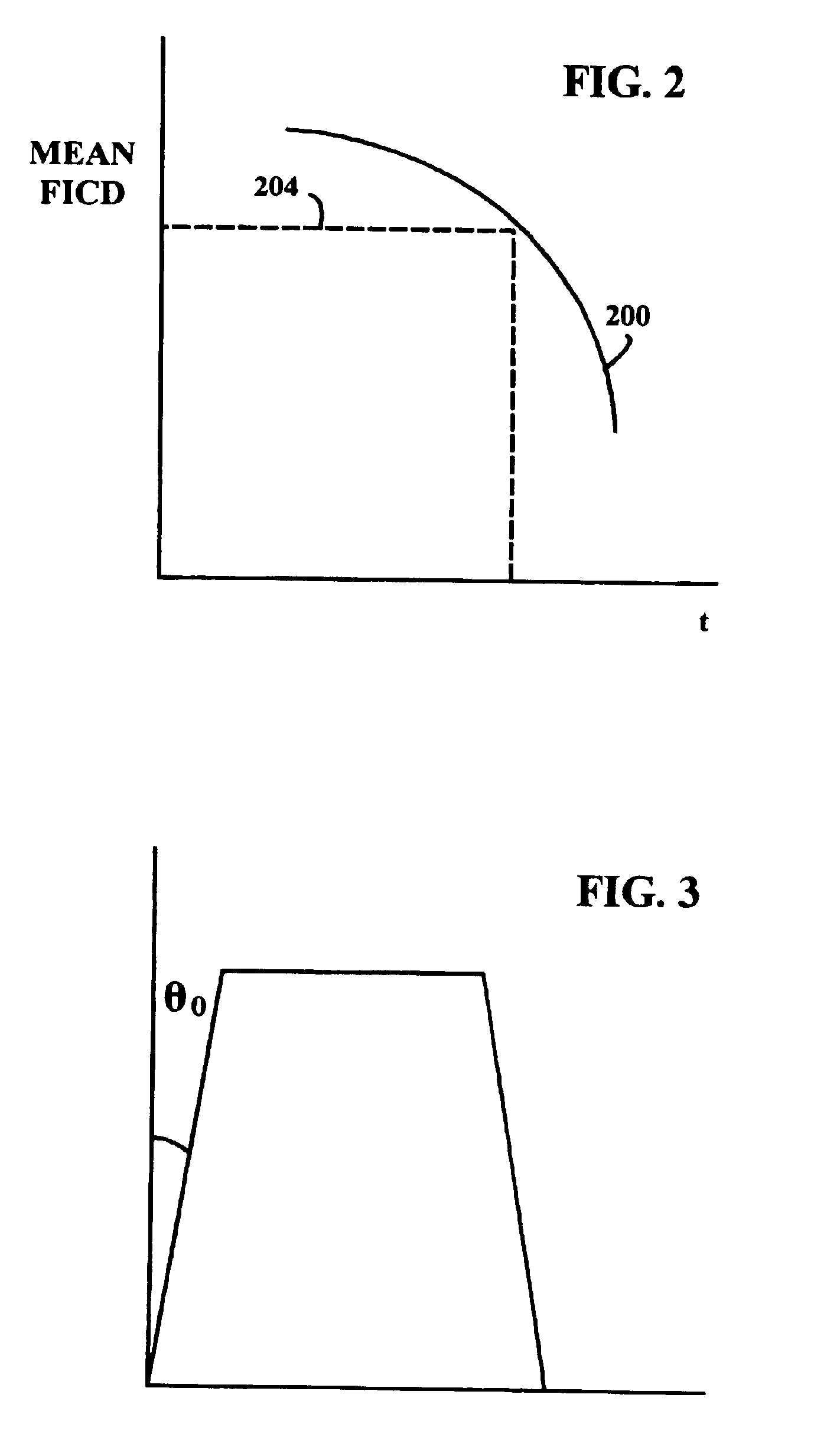
Figure 3
Abstract
Description
BACKGROUND OF THE INVENTION
[0001] 1. Field of the Invention
[0002] The present invention relates to semiconductor fabrication methods. More precisely, the present invention relates to a control system used in semiconductor fabrication for controlling feature critical dimensions.
[0003] 2. Description of the Related Art
[0004] Two aspects of feature sizes are controlled in a lithographic and etch process. The first aspect is a critical dimension, the absolute size of a feature, including linewidth, spacing or contact dimensions. The second aspect is the variation in feature size across the wafer surface as measured by steps of a wafer stepper. Linewidth and spacing measurements are regularly performed to determine the actual sizes of critical dimensions at each masking level of a process.
[0005] Another aspect of linewidth control is that correct feature sizes are to be maintained across an entire wafer and also maintained from wafer to wafer. As a feature size is reduced, the tolerable error...
Examples
Embodiment Construction
[0023]Referring to FIG. 1, a flow chart illustrates a control method for controlling critical dimensions in a semiconductor fabrication process 100 by adjusting the fabrication parameters or “recipe” for a photoresist etch step 106 previous to a polysilicon gate etch step in the fabrication process 100. In particular, the critical dimensions are controlled using photoresist etch time as a control variable to drive the critical dimensions to a target value.
[0024]In overview, the fabrication process 100 involves selection of one or more test wafers, called “pilot” wafers from an entire lot of wafers. The pilot wafers are tested to characterize the lot of wafers, processed through the photoresist etch step 106 using a nominal, average, or moving average processing recipe, and measured in a Final Inspection Critical Dimensions step 108. The results from the pilot lot tests are applied to update a process model 114 which is used to adjust the etch recipe for the remaining wafers in the l...