

Benchmarking RRAM Performance: Speed, Scalability, Lifespan
SEP 10, 20259 MIN READ
Generate Your Research Report Instantly with AI Agent
PatSnap Eureka helps you evaluate technical feasibility & market potential.
RRAM Technology Evolution and Performance Objectives
Resistive Random Access Memory (RRAM) has emerged as a promising non-volatile memory technology over the past two decades, evolving from theoretical concepts to commercial prototypes. The technology leverages resistance switching phenomena in various metal oxide materials, with early research dating back to the 1960s. However, significant breakthroughs in the early 2000s catalyzed accelerated development, particularly when researchers demonstrated reliable resistance switching in simple metal-insulator-metal structures.
The evolution of RRAM technology has been marked by several key milestones. Initially, the focus was on proving the fundamental switching mechanism, followed by material optimization to improve retention and endurance characteristics. By the 2010s, research shifted toward scaling capabilities, with demonstrations of devices below 10nm showing RRAM's potential compatibility with advanced technology nodes. Recent developments have concentrated on multi-level cell capabilities and 3D integration approaches to increase storage density.
Current performance benchmarks for RRAM indicate switching speeds in the nanosecond range, with some experimental devices achieving sub-nanosecond operation. This positions RRAM favorably compared to NAND flash (microseconds) but still behind DRAM (picoseconds). Endurance specifications have improved from early demonstrations of 10^4-10^6 cycles to recent reports exceeding 10^12 cycles in optimized structures, approaching the requirements for DRAM replacement applications.
The scalability trajectory of RRAM has been particularly impressive, with functional devices demonstrated at dimensions below 5nm. This scaling capability outperforms many competing non-volatile memory technologies and suggests compatibility with future semiconductor process nodes. Power consumption metrics have also improved substantially, with operating currents reduced from hundreds of microamperes to sub-microampere levels in advanced selector-based architectures.
The primary technical objectives for RRAM development focus on three critical performance dimensions: speed, scalability, and lifespan. Speed objectives include achieving write/read operations below 1ns to compete with volatile memories while maintaining non-volatility. Scalability goals target reliable operation at 2nm technology nodes and below, with particular emphasis on maintaining performance consistency at these dimensions. Lifespan objectives aim to demonstrate endurance exceeding 10^15 cycles and retention beyond 10 years at 85°C to meet enterprise storage requirements.
Additional performance objectives include reducing device-to-device variability below 5%, decreasing operating voltages under 1V for mobile applications, and demonstrating multi-level cell capabilities with at least 3 bits per cell to maximize storage density. These targets collectively define the roadmap for RRAM to transition from a promising technology to a mainstream memory solution capable of addressing the growing demands of data-intensive computing paradigms.
Market Demand Analysis for Next-Generation Memory Solutions
The memory technology landscape is experiencing a significant shift as traditional solutions reach their physical limitations. The global market for next-generation memory technologies is projected to reach $27.6 billion by 2025, growing at a CAGR of 29.7% from 2020. This growth is primarily driven by increasing demands for higher performance, lower power consumption, and greater storage density across multiple industries.
Resistive Random Access Memory (RRAM) has emerged as a promising candidate among emerging memory technologies, with market analysts forecasting its segment to grow at 35.2% CAGR through 2026. This accelerated growth reflects the technology's potential to address critical limitations in current memory solutions while offering superior performance characteristics.
Data-intensive applications are creating unprecedented demand for memory solutions that can process information at higher speeds. The explosion of artificial intelligence and machine learning workloads requires memory architectures capable of handling massive parallel operations with minimal latency. RRAM's switching speed in the nanosecond range positions it favorably against competing technologies like PCRAM (phase-change memory) and MRAM (magnetoresistive RAM).
The Internet of Things (IoT) ecosystem represents another significant market driver, with an estimated 75 billion connected devices expected by 2025. These edge devices require memory solutions that combine high performance with extreme energy efficiency. RRAM's non-volatile nature and low power consumption make it particularly suitable for battery-powered and energy-harvesting IoT applications.
Automotive and industrial sectors are increasingly demanding memory solutions that can withstand harsh operating environments. The automotive memory market alone is expected to grow at 23.9% CAGR through 2026, with advanced driver-assistance systems (ADAS) and autonomous vehicles requiring robust, high-endurance memory technologies. RRAM's potential for high temperature operation and radiation hardness addresses these specialized requirements.
Mobile and consumer electronics continue to drive significant memory demand, with manufacturers seeking solutions that enable thinner devices with longer battery life. The scalability advantages of RRAM could potentially allow for higher storage densities in smaller form factors, addressing a critical pain point in portable device design.
Enterprise storage systems are transitioning toward memory-centric architectures that can overcome the traditional bottlenecks between processing and storage. The storage class memory market is projected to reach $17.9 billion by 2025, with RRAM positioned as a potential bridge between DRAM's performance and NAND flash's capacity and cost structure.
RRAM Development Status and Technical Barriers
Resistive Random Access Memory (RRAM) technology has emerged as a promising candidate for next-generation non-volatile memory solutions. Currently, RRAM development has reached a critical juncture where commercial viability is being actively pursued by major semiconductor manufacturers and research institutions worldwide. Laboratory demonstrations have shown impressive performance metrics, with switching speeds in the nanosecond range, endurance cycles exceeding 10^9, and retention times of over 10 years at elevated temperatures.
Despite these achievements, significant technical barriers persist in RRAM development. The foremost challenge involves the trade-off between performance parameters - improving one metric often degrades others. For instance, enhancing switching speed typically compromises retention time, while optimizing endurance may impact reliability. This fundamental tension has prevented RRAM from achieving the balanced performance profile necessary for widespread commercial adoption.
Material stability represents another critical barrier, as many RRAM devices suffer from compositional changes during repeated cycling. The migration of oxygen vacancies and metal ions, which enables the resistive switching mechanism, also contributes to device degradation over time. This manifests as resistance drift, where the high and low resistance states gradually converge, reducing the sensing margin and ultimately leading to read errors.
Scalability challenges present significant obstacles as device dimensions approach sub-20nm nodes. At these scales, variability in switching behavior increases dramatically due to the stochastic nature of filament formation. This cell-to-cell and cycle-to-cycle variability complicates the design of reliable sensing circuits and error correction mechanisms, limiting integration density and yield in large arrays.
Power consumption during write operations remains substantially higher than competing technologies, with typical SET/RESET voltages ranging from 1-3V. This creates thermal management challenges in high-density arrays and limits RRAM's applicability in ultra-low-power applications such as IoT edge devices and energy harvesting systems.
Manufacturing integration presents additional hurdles, particularly regarding compatibility with standard CMOS processes. While some RRAM technologies can be integrated in the back-end-of-line (BEOL), others require specialized materials or processing conditions that complicate fabrication and increase costs. The lack of standardization across different RRAM technologies further fragments development efforts and slows industry-wide adoption.
Addressing these technical barriers requires coordinated research across multiple disciplines, including materials science, device physics, circuit design, and manufacturing engineering. Recent innovations in engineered switching layers, novel electrode materials, and optimized programming schemes show promise in overcoming these limitations, potentially unlocking RRAM's full potential as a universal memory solution.
Current RRAM Benchmarking Methodologies and Standards
01 RRAM Speed and Switching Characteristics
RRAM devices demonstrate high-speed operation capabilities, with switching times in the nanosecond range. The resistive switching mechanism allows for rapid transitions between high and low resistance states, enabling fast read and write operations. The speed performance is influenced by the composition of the switching layer and electrode materials. Advanced designs incorporate optimized switching materials and interface engineering to reduce switching delay and improve overall operational speed.- RRAM Speed and Switching Characteristics: RRAM devices demonstrate high-speed operation capabilities with fast switching between resistance states. The switching speed is typically in the nanosecond range, making them suitable for high-performance computing applications. The rapid transition between high and low resistance states is achieved through controlled ion migration within the resistive switching layer. This fast switching characteristic enables RRAM to compete with traditional volatile memory technologies while maintaining non-volatile data storage capabilities.
- Scalability and Integration Density of RRAM: RRAM offers excellent scalability potential, allowing for high-density memory arrays. The simple two-terminal structure of RRAM cells enables smaller feature sizes compared to conventional memory technologies. Cross-point architectures can be implemented to achieve 3D stacking, significantly increasing storage density. The scalability of RRAM makes it particularly promising for applications requiring high storage capacity in limited physical space, such as mobile devices and embedded systems.
- RRAM Endurance and Lifespan Enhancement: The endurance and lifespan of RRAM devices are critical factors affecting their commercial viability. Various approaches have been developed to enhance RRAM endurance, including optimized material selection, interface engineering, and improved switching protocols. Current RRAM technologies can achieve endurance levels ranging from 10^6 to 10^12 switching cycles, depending on the materials and structures used. Techniques such as pulse width modulation and voltage amplitude control can significantly extend the operational lifespan of RRAM devices.
- Material Innovations for RRAM Performance: Material selection plays a crucial role in determining RRAM performance characteristics. Various oxide materials, including HfOx, TaOx, and TiOx, have been investigated as switching layers. The interface between the electrode and switching layer significantly impacts device performance. Doping strategies and multi-layer structures have been developed to optimize switching behavior, reduce variability, and enhance reliability. Novel materials such as 2D materials and nanocomposites are being explored to further improve RRAM performance metrics.
- RRAM Architecture and Circuit Design: Advanced architectures and circuit designs are essential for maximizing RRAM performance. Cross-point arrays, selector devices, and sensing circuits have been developed to address issues such as sneak path currents and read disturbances. Innovative programming schemes help balance speed, energy efficiency, and reliability. Hybrid memory systems combining RRAM with conventional memory technologies leverage the strengths of each technology. These architectural innovations are crucial for realizing the full potential of RRAM in practical applications.
02 Scalability and Miniaturization of RRAM
RRAM technology offers excellent scalability potential, allowing for device dimensions to be reduced to nanometer scale. The simple two-terminal structure facilitates high-density integration and 3D stacking capabilities. Scaling advantages include reduced power consumption, increased storage density, and compatibility with conventional CMOS processes. Various approaches to improve scalability include novel cell architectures, material innovations, and advanced fabrication techniques that maintain performance integrity at smaller dimensions.Expand Specific Solutions03 RRAM Endurance and Lifespan Enhancement
The lifespan of RRAM devices is characterized by their endurance, which refers to the number of write/erase cycles they can withstand before failure. Various techniques have been developed to enhance RRAM endurance, including optimized pulse programming schemes, interface engineering, and doping of the resistive switching layer. Innovations in material composition and device structure have led to significant improvements in cycle lifetime, with some designs achieving endurance of over 10^9 cycles.Expand Specific Solutions04 Material Innovations for RRAM Performance
Material selection plays a crucial role in determining RRAM performance characteristics. Various oxide materials, including transition metal oxides, have been investigated for the resistive switching layer. The electrode materials and their interfaces with the switching layer significantly impact device operation. Novel material systems, such as two-dimensional materials, nanocomposites, and engineered defect structures, have been developed to optimize the speed-endurance-retention tradeoff in RRAM devices.Expand Specific Solutions05 RRAM Architecture and Integration Solutions
Advanced RRAM architectures have been developed to address integration challenges and improve overall system performance. These include crossbar arrays, 3D stacking configurations, and hybrid memory systems. Integration solutions focus on addressing sneak path issues, reducing parasitic effects, and ensuring compatibility with peripheral circuitry. Novel selector devices and programming schemes have been implemented to enable high-density memory arrays while maintaining reliable operation and addressing the speed-power-density tradeoffs.Expand Specific Solutions
Leading Companies and Research Institutions in RRAM Field
The RRAM (Resistive Random Access Memory) market is currently in a growth phase, with increasing adoption across various applications due to its advantages in speed, scalability, and power efficiency. The global RRAM market is projected to expand significantly, driven by demand for faster, more energy-efficient memory solutions. In terms of technical maturity, major semiconductor manufacturers like Samsung, Intel, Micron, and TSMC are leading commercial development, while research institutions such as National University of Singapore and Chinese Academy of Sciences are advancing fundamental innovations. Companies including KIOXIA, GlobalFoundries, and Huawei are investing heavily in RRAM technology to overcome endurance limitations and manufacturing challenges. The competitive landscape features both established memory giants and specialized startups like SuperMem, with increasing collaboration between industry and academic institutions to accelerate commercialization.
Taiwan Semiconductor Manufacturing Co., Ltd.
Technical Solution: TSMC has developed embedded RRAM (eRRAM) technology optimized for logic integration in advanced process nodes. Their benchmarking approach focuses on manufacturability and integration with logic processes rather than standalone memory performance. TSMC's RRAM technology demonstrates switching speeds of 10-50ns and endurance of 10^6-10^8 cycles depending on the specific implementation. The company has pioneered backend-of-line (BEOL) integration techniques that allow RRAM cells to be fabricated between metal interconnect layers, enabling high-density memory without sacrificing silicon area for logic. Their benchmarking methodology includes comprehensive variability analysis across wafers and lots to ensure manufacturing consistency. TSMC has implemented innovative forming-free RRAM cells that eliminate the need for high-voltage initialization, simplifying peripheral circuitry and improving reliability. Their technology shows particular strength in IoT and edge computing applications where power efficiency and integration density are critical.
Strengths: Excellent CMOS compatibility enabling seamless logic integration; low-temperature processing compatible with advanced nodes; superior area efficiency compared to embedded flash. Weaknesses: Limited endurance compared to dedicated memory technologies; performance variability across process corners; higher access latency compared to SRAM alternatives.
Samsung Electronics Co., Ltd.
Technical Solution: Samsung has developed proprietary RRAM technology focusing on ultra-high density and scalability for next-generation memory applications. Their vertical RRAM (vRRAM) architecture enables 3D stacking of memory cells, significantly increasing storage density while maintaining acceptable switching speeds. Samsung's benchmarking methodology is particularly comprehensive, evaluating performance across multiple parameters including switching speed (achieving sub-50ns switching), data retention (>10 years at 85°C), and endurance (>10^9 cycles for select configurations). The company has implemented innovative material stacks including hafnium oxide-based switching layers with engineered oxygen vacancy distributions to optimize performance. Their testing protocols include accelerated lifetime testing and statistical analysis of cell-to-cell and cycle-to-cycle variations to ensure reliability in mass production. Samsung has also developed specialized peripheral circuits that optimize programming conditions for each cell, reducing variability and extending device lifespan.
Strengths: Industry-leading manufacturing capabilities enabling rapid scaling and commercialization; excellent retention characteristics at small technology nodes; strong integration with existing memory hierarchies. Weaknesses: Higher programming voltages compared to some competitors; cycle-to-cycle variability requiring sophisticated error correction; challenges with uniform switching behavior in high-density arrays.
Critical Patents and Research on RRAM Speed and Endurance
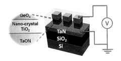
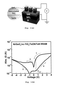
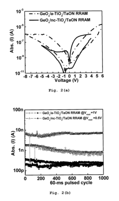
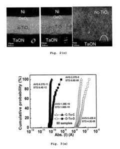
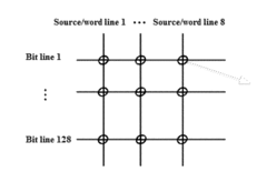
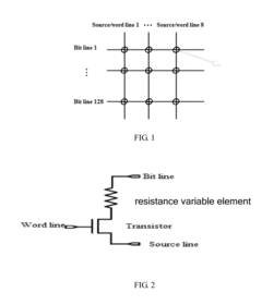
Resistive random access memory (RRAM) using stacked dielectrics and method for manufacturing the same
PatentInactiveUS20130126818A1
Innovation
- A RRAM device with a metal-insulator-metal (MIM) structure using stacked dielectrics of GeOx/nc-TiO2/TaON and different work-function top and bottom electrodes, achieving ultra-low switching energy and extremely long endurance through the use of Ni/GeOx/nc-TiO2/TaN structure with low-cost electrodes, resulting in a large resistance window, good switching uniformity, and cycling endurance up to 5×10^9 cycles.
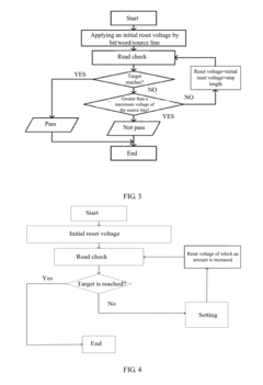
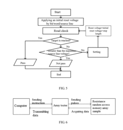
Operation Method of Resistive Random Access Memory and Resistive Random Access Memory Device
PatentActiveUS20180330788A1
Innovation
- An operation method for RRAM that involves applying an initial reset voltage, performing a read check to determine if the resistance value reaches a preset target resistance value, and iteratively adjusting the voltage to maintain the storage unit in a low resistance state before resetting, ensuring the resistance value reaches the target high resistance state, thereby preventing rapid relaxation.
Material Science Innovations for RRAM Scalability
Material science innovations represent a critical frontier in advancing RRAM (Resistive Random Access Memory) technology toward greater scalability. The fundamental challenge lies in identifying and engineering materials that can maintain reliable resistive switching behaviors at increasingly smaller dimensions while supporting high-density integration requirements.
Recent breakthroughs in oxide-based materials have demonstrated promising results for RRAM scalability. Hafnium oxide (HfO2) and tantalum oxide (Ta2O5) have emerged as leading candidates due to their excellent compatibility with CMOS processes and ability to maintain stable switching characteristics at sub-10nm feature sizes. These materials exhibit favorable conduction mechanisms that remain consistent even as device dimensions shrink.
Metal-oxide interfaces have become a particular focus of innovation, with researchers developing novel bilayer and multilayer structures that enhance filament formation control. For instance, HfO2/Ta2O5 bilayer structures have demonstrated improved uniformity in resistive switching compared to single-layer alternatives, enabling more predictable performance as devices scale down to smaller nodes.
Doping strategies represent another promising avenue for enhancing RRAM scalability. Introducing specific elements such as titanium, aluminum, or nitrogen into oxide matrices has been shown to modify defect concentrations and oxygen vacancy distributions, resulting in more controlled filament formation. These approaches have yielded devices with reduced variability and improved retention characteristics at smaller dimensions.
Two-dimensional materials, including graphene and transition metal dichalcogenides (TMDs), are being explored as potential game-changers for ultra-scaled RRAM. Their atomically thin nature provides inherent advantages for extreme scaling scenarios, with recent demonstrations showing functional RRAM cells incorporating MoS2 barriers achieving switching areas below 10nm2 while maintaining distinguishable resistance states.
Interface engineering techniques have also advanced significantly, with atomic layer deposition (ALD) and molecular beam epitaxy (MBE) enabling precise control over material interfaces at the atomic scale. These techniques allow for the creation of engineered defect profiles that can guide filament formation pathways even in highly scaled devices, addressing one of the key challenges in maintaining reliable operation at smaller dimensions.
The integration of these material innovations with advanced fabrication techniques presents a promising pathway toward RRAM devices that maintain performance integrity while scaling to dimensions compatible with future technology nodes, potentially enabling memory densities that approach or exceed those of established technologies like NAND flash.
Integration Challenges with Conventional CMOS Technology
The integration of Resistive Random Access Memory (RRAM) with conventional CMOS technology presents significant challenges despite its promising performance characteristics in terms of speed, scalability, and lifespan. One of the primary obstacles is the material compatibility issue between RRAM's metal oxide layers and standard CMOS processes. The high-temperature annealing steps in CMOS fabrication can degrade RRAM's resistive switching materials, compromising their performance and reliability.
Process integration complexity also poses substantial challenges. RRAM typically requires additional processing steps beyond standard CMOS flows, including specialized deposition techniques for metal oxide layers and precise control of oxygen vacancy concentrations. These extra steps increase manufacturing complexity and potentially reduce yield, affecting cost-effectiveness of the integrated solution.
Electrical interface compatibility represents another critical challenge. RRAM cells operate at voltage levels that may differ from standard CMOS logic, necessitating specialized interface circuits. These circuits must efficiently translate between RRAM's resistive switching behavior and CMOS logic levels while minimizing power consumption and maintaining signal integrity across the interface boundary.
Scaling issues emerge when attempting to integrate high-density RRAM arrays with advanced CMOS nodes. As CMOS technology scales down to sub-10nm nodes, the dimensional mismatch between RRAM cells and transistor features becomes more pronounced. This mismatch complicates 3D integration efforts and limits the potential density advantages of RRAM technology.
Reliability concerns arise from the interaction between RRAM's switching mechanisms and CMOS transistor characteristics. Voltage stress from RRAM programming operations can accelerate transistor aging effects such as bias temperature instability and hot carrier injection, potentially reducing the overall system lifespan below acceptable levels for commercial applications.
Thermal management presents yet another integration challenge. RRAM programming operations generate localized heating that can affect nearby CMOS components, potentially causing parameter drift or accelerated aging. Effective thermal isolation structures must be incorporated into the integrated design, adding further complexity to the manufacturing process.
Industry standardization remains incomplete for RRAM-CMOS integration, with multiple competing approaches and limited consensus on optimal integration strategies. This fragmentation slows adoption and complicates the development of design tools and manufacturing processes that could address the aforementioned challenges systematically.
Unlock deeper insights with PatSnap Eureka Quick Research — get a full tech report to explore trends and direct your research. Try now!
Generate Your Research Report Instantly with AI Agent
Supercharge your innovation with PatSnap Eureka AI Agent Platform!