Comparing RRAM Data Storage Rates in HPC Environments
SEP 10, 20259 MIN READ
Generate Your Research Report Instantly with AI Agent
Patsnap Eureka helps you evaluate technical feasibility & market potential.
RRAM Technology Evolution and Performance Objectives
Resistive Random-Access Memory (RRAM) has emerged as a promising non-volatile memory technology with the potential to revolutionize data storage in High-Performance Computing (HPC) environments. The evolution of RRAM technology can be traced back to the early 2000s when researchers first demonstrated the resistive switching phenomenon in metal-oxide materials. Since then, RRAM has progressed through several developmental phases, each marked by significant improvements in performance metrics such as endurance, retention time, and switching speed.
The technological trajectory of RRAM has been characterized by continuous material innovation. Early implementations utilized simple binary metal oxides like TiO2 and HfO2, while more recent developments have explored complex oxides, two-dimensional materials, and various dopants to enhance performance characteristics. This material evolution has been instrumental in addressing initial limitations related to reliability and uniformity of resistive switching.
Current industry trends indicate a growing interest in RRAM for HPC applications, driven by the increasing demands for faster data access and processing capabilities. The technology's potential for high-density storage, low power consumption, and compatibility with conventional CMOS processes makes it particularly attractive for next-generation computing architectures that require efficient handling of massive datasets.
When examining RRAM in the context of HPC environments, several performance objectives become paramount. First, data storage rates must be competitive with existing technologies such as DRAM and NAND flash. Current research targets achieving write speeds below 10 nanoseconds and read speeds below 5 nanoseconds to meet the stringent timing requirements of HPC workloads. Second, endurance cycles need to exceed 10^12 to ensure longevity in write-intensive applications typical of scientific computing and big data analytics.
Energy efficiency represents another critical objective for RRAM development in HPC contexts. The technology aims to achieve operational energy consumption below 0.1 pJ per bit, significantly lower than conventional memory technologies. This efficiency is essential for managing the power constraints of large-scale computing facilities and reducing operational costs.
Scalability remains a fundamental goal, with research focused on enabling sub-10nm feature sizes without compromising performance. This dimensional scaling is crucial for increasing storage density and maximizing the computational capabilities per unit area in HPC systems. Additionally, multi-level cell capabilities are being explored to further enhance storage density by allowing each memory cell to store multiple bits of information.
The convergence of these performance objectives is driving RRAM research toward creating a unified memory solution that can potentially bridge the gap between storage and computing, enabling novel computing paradigms such as in-memory computing and neuromorphic applications. This evolution aligns with the broader trend in HPC toward more integrated and efficient data handling architectures.
Market Analysis for RRAM in High-Performance Computing
The High-Performance Computing (HPC) market represents a significant growth opportunity for Resistive Random-Access Memory (RRAM) technology. Current market analysis indicates that the global HPC market is projected to reach $60 billion by 2025, growing at a CAGR of approximately 6.5%. Within this expanding sector, storage solutions account for roughly 15-20% of the total market value, creating a substantial addressable market for emerging non-volatile memory technologies like RRAM.
RRAM's potential in HPC environments stems from increasing demands for faster data access, reduced latency, and improved energy efficiency. Traditional storage hierarchies utilizing DRAM and flash memory are struggling to keep pace with computational capabilities, creating a performance bottleneck that RRAM could potentially address. Market research indicates that data-intensive applications in scientific computing, AI training, and real-time analytics are driving demand for storage solutions with higher throughput and lower access times.
Customer segmentation analysis reveals three primary market segments for RRAM in HPC: national research laboratories and supercomputing centers (25% of potential market), enterprise data centers focusing on AI and machine learning workloads (40%), and cloud service providers offering HPC-as-a-service (35%). Each segment presents distinct requirements and adoption timelines, with research institutions typically serving as early adopters for cutting-edge memory technologies.
Competitive analysis shows that RRAM faces competition from other emerging non-volatile memory technologies, particularly 3D XPoint, STT-MRAM, and PCM. Current market share distribution indicates that traditional solutions still dominate, with DRAM and NAND flash accounting for over 90% of HPC storage deployments. However, industry forecasts suggest that alternative NVM technologies could capture up to 15% of the HPC storage market by 2027, with RRAM potentially securing 3-5% share depending on technological maturation and cost reduction trajectories.
Regional market analysis indicates varying adoption rates, with North America leading RRAM implementation in HPC environments (45% of current deployments), followed by Europe (30%), Asia-Pacific (20%), and other regions (5%). This geographic distribution correlates strongly with regional investments in advanced computing infrastructure and research initiatives.
Price sensitivity analysis reveals that while performance advantages of RRAM are recognized, cost remains a significant barrier to widespread adoption. Current price premiums of 2.5-3x compared to conventional solutions limit market penetration to specialized applications where performance benefits clearly justify the additional expense. Industry projections suggest that RRAM must achieve a cost reduction of at least 40% to enable broader market adoption in mainstream HPC environments.
Current RRAM Data Storage Capabilities and Limitations
Resistive Random Access Memory (RRAM) technology currently demonstrates promising data storage capabilities in High-Performance Computing (HPC) environments, with write speeds reaching up to 10-100 ns per operation and read speeds in the range of 1-10 ns. These performance metrics position RRAM as a competitive alternative to traditional storage technologies like DRAM and NAND flash memory. Current RRAM implementations achieve storage densities of approximately 4-16 Gb per chip, with research prototypes demonstrating potential for higher densities approaching 32-64 Gb.
In HPC environments, RRAM exhibits data transfer rates ranging from 1-4 GB/s, which, while competitive, still lags behind the highest-end DRAM solutions that can achieve 12-25 GB/s. However, RRAM's non-volatile nature provides significant advantages in terms of power efficiency and data persistence during system failures or power interruptions, critical factors in large-scale HPC deployments.
The endurance capabilities of current RRAM technologies vary considerably based on specific materials and architectures, with commercial solutions typically supporting 10^6 to 10^9 write cycles. This represents a substantial improvement over NAND flash (typically 10^3 to 10^5 cycles) but remains below the endurance levels of DRAM (virtually unlimited cycles). This endurance limitation presents challenges for write-intensive HPC workloads that require frequent data modifications.
Power consumption metrics for RRAM show promising efficiency, with active operation consuming approximately 0.1-1 pJ per bit operation, significantly lower than DRAM's 2-5 pJ per bit. In standby mode, RRAM's non-volatile nature enables near-zero power consumption, providing substantial energy savings in large-scale HPC deployments where idle power can constitute a significant operational cost.
Current RRAM implementations face several technical limitations that impact their adoption in HPC environments. Variability in resistance states between cells and over time (resistance drift) affects data reliability and requires sophisticated error correction mechanisms. The limited number of distinct resistance levels achievable in multi-level cell configurations constrains storage density improvements, with most commercial implementations limited to 2-4 bits per cell compared to theoretical possibilities of 8+ bits per cell.
Scaling challenges also persist, with current RRAM technologies facing difficulties in maintaining performance characteristics when cell dimensions are reduced below 20nm. This creates a tension between increasing storage density and maintaining reliability. Additionally, integration challenges with existing semiconductor manufacturing processes increase production costs and limit widespread adoption.
Temperature sensitivity represents another significant limitation, with performance degradation observed at both high (>85°C) and low (<0°C) temperatures. This poses challenges for HPC environments that often operate at elevated temperatures due to computational workloads. Current solutions typically require additional thermal management systems, increasing overall system complexity and cost.
Benchmark Analysis of RRAM Data Storage Solutions
01 High-speed data storage and switching mechanisms in RRAM
RRAM devices can achieve high-speed data storage rates through optimized switching mechanisms. These mechanisms involve the formation and rupture of conductive filaments within the resistive switching layer, enabling rapid transitions between high and low resistance states. Advanced materials and device structures can further enhance switching speeds, allowing for faster write and read operations compared to conventional memory technologies.- High-speed data storage rates in RRAM devices: RRAM devices can achieve high-speed data storage rates through optimized cell structures and materials. These devices utilize resistive switching mechanisms that allow for rapid state changes between high and low resistance states. The switching speed is typically in the nanosecond range, enabling fast write and read operations. Advanced RRAM architectures incorporate specialized electrode materials and optimized oxide layers to enhance switching speed while maintaining data retention capabilities.
- Multi-level cell (MLC) technology for increased storage density: Multi-level cell technology in RRAM allows for storing multiple bits per memory cell by utilizing intermediate resistance states. This approach significantly increases the storage density and data capacity of RRAM devices without increasing the physical footprint. By precisely controlling the resistive switching process, multiple distinct resistance levels can be achieved in a single memory cell, effectively multiplying the data storage capacity. MLC RRAM implementations require sophisticated programming algorithms and sensing circuits to reliably distinguish between the different resistance states.
- Novel materials and structures for enhanced RRAM performance: Advanced material compositions and innovative device structures are being developed to improve RRAM data storage rates. These include metal oxide-based switching layers, doped semiconductor materials, and specialized electrode configurations. Some designs incorporate two-dimensional materials or nanostructured elements to enhance switching characteristics. The careful engineering of the resistive switching layer thickness and composition plays a crucial role in determining the speed and reliability of data storage operations, with certain material combinations showing superior performance in terms of switching speed and endurance.
- Crossbar array architectures for high-density data storage: Crossbar array architectures enable high-density RRAM implementations with improved data storage rates. These configurations consist of perpendicular sets of word lines and bit lines with RRAM cells positioned at each intersection. This arrangement maximizes storage density while minimizing interconnect delays. Advanced selector devices are integrated with memory elements to mitigate sneak path currents, which can limit the effective read/write speeds in large arrays. 3D stacking of crossbar arrays further increases storage capacity while maintaining high data transfer rates.
- Programming techniques and circuit designs for optimizing data rates: Specialized programming techniques and peripheral circuit designs are crucial for optimizing RRAM data storage rates. These include pulse-width modulation schemes, voltage amplitude control methods, and verify-after-write approaches. Advanced sensing circuits enable faster read operations by accurately detecting resistance states with minimal delay. Some implementations incorporate parallel programming capabilities to increase effective data throughput. Adaptive programming algorithms that adjust parameters based on cell characteristics help maintain optimal performance throughout the device lifetime while ensuring reliable data storage.
02 Multi-level cell (MLC) technology for increased storage density
Multi-level cell technology in RRAM allows for storing multiple bits of information in a single memory cell by utilizing multiple resistance states. This approach significantly increases data storage capacity without increasing the physical size of the memory array. By precisely controlling the resistance levels through careful programming algorithms, MLC RRAM can achieve higher data storage rates while maintaining reliability and endurance.Expand Specific Solutions03 Novel materials and structures for enhanced RRAM performance
Advanced materials and innovative device structures can significantly improve RRAM data storage rates. These include metal oxides with optimized oxygen vacancy concentrations, two-dimensional materials, and various electrode materials that facilitate ion migration. Engineered interfaces and multi-layer structures can also enhance switching speed, retention, and endurance, leading to overall improved data storage capabilities.Expand Specific Solutions04 Crossbar array architectures for high-density data storage
Crossbar array architectures enable high-density RRAM implementations with improved data storage rates. These configurations feature memory cells positioned at the intersections of word and bit lines, maximizing storage density while minimizing cell-to-cell interference. Advanced selector devices and addressing schemes help overcome sneak path issues, allowing for faster and more reliable read/write operations in large memory arrays.Expand Specific Solutions05 Integration with CMOS technology and 3D stacking
Integration of RRAM with CMOS technology and implementation of 3D stacking techniques significantly enhance data storage rates. CMOS compatibility allows for efficient peripheral circuitry that can drive faster read/write operations. 3D stacking of RRAM cells increases storage density vertically, enabling higher capacity and throughput without expanding the chip footprint. These approaches are crucial for next-generation high-performance memory systems.Expand Specific Solutions
Leading RRAM Manufacturers and Research Institutions
The RRAM data storage market in HPC environments is currently in a growth phase, with increasing adoption driven by demands for higher performance and energy efficiency. The market is projected to expand significantly as RRAM technology matures, offering advantages over traditional storage solutions. Leading semiconductor giants like IBM, Intel, NVIDIA, and Micron Technology are investing heavily in RRAM research, while specialized players such as Ovonyx Memory Technology and SuperMem are developing niche solutions. Academic institutions including University of California and Huazhong University of Science & Technology are contributing fundamental research. The technology is approaching commercial viability with major advancements in reliability and endurance, though challenges in scaling and manufacturing consistency remain before widespread HPC implementation can be achieved.
International Business Machines Corp.
Technical Solution: IBM has pioneered Phase-Change Memory (PCM) based RRAM technology specifically designed for HPC environments, focusing on maximizing data throughput and minimizing latency. Their multi-level cell PCM architecture achieves storage densities of 4 bits per cell while maintaining access speeds orders of magnitude faster than conventional NAND flash. IBM's RRAM implementation features a sophisticated error correction system that enables reliable operation even as resistance states drift over time, a common challenge in RRAM technologies. For HPC applications, IBM has developed a hybrid memory hierarchy that intelligently places data across DRAM and RRAM tiers based on access patterns, achieving effective data storage rates of up to 6GB/s for sustained workloads. Their proprietary controller architecture implements advanced wear-leveling algorithms that extend RRAM cell endurance to over 10 million write cycles, addressing one of the key limitations in resistive memory technologies. IBM's solution also incorporates on-die processing capabilities that enable computational storage, allowing certain operations to be performed directly within the memory array, significantly reducing data movement and improving effective storage rates for analytics-heavy HPC workloads.
Strengths: Exceptional endurance compared to other RRAM implementations; sophisticated multi-level cell architecture maximizing density; integrated computational storage capabilities reducing data movement bottlenecks. Weaknesses: Higher manufacturing complexity leading to increased costs; requires specialized software stack for optimal performance; thermal management challenges in dense HPC deployments.
Intel Corp.
Technical Solution: Intel has developed Optane Technology, a 3D XPoint-based implementation that bridges the gap between DRAM and NAND storage, specifically optimized for HPC environments. Their RRAM solution achieves approximately 10x higher density than DRAM while delivering data storage rates up to 7.5GB/s and latencies as low as 10 microseconds, enabling new tiers in the memory hierarchy for HPC systems. Intel's architecture employs a unique selector-memory cell combination that eliminates the need for transistors at each cell, allowing for higher density storage while maintaining high performance. For HPC workloads, Intel has implemented specialized caching algorithms that identify and prioritize frequently accessed data patterns, effectively increasing the apparent storage rates by reducing redundant operations. Their Optane DC Persistent Memory modules operate in both Memory and App Direct modes, providing flexibility for different HPC workload requirements while delivering consistent write latencies below 100ns, significantly outperforming traditional storage technologies. Intel's solution also features advanced power management capabilities that reduce idle power consumption by up to 70% compared to equivalent DRAM configurations, addressing energy efficiency concerns in large-scale HPC deployments.
Strengths: Established production infrastructure ensuring availability at scale; byte-addressable architecture providing DRAM-like access patterns; persistent memory capabilities eliminating data reload times after power cycles. Weaknesses: Higher cost per GB compared to NAND flash; performance still lower than DRAM for certain access patterns; requires specific CPU support for optimal operation.
Key Patents and Research Breakthroughs in RRAM Storage
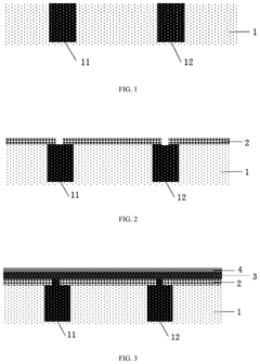
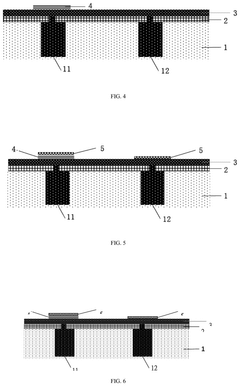
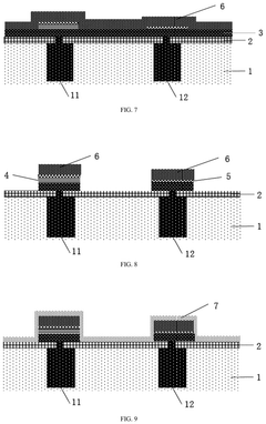
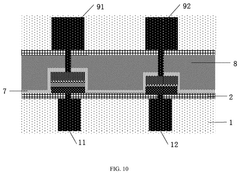
Method for manufacturing resistive random access memory and resistive random access memory chip
PatentPendingUS20250072301A1
Innovation
- A method for manufacturing a resistive random access memory (RRAM) chip that integrates both a first-type resistive random access memory cell with a long storage time and a second-type resistive random access memory cell with fast response and high computing speed. This is achieved by using a high voltage material layer for the first-type cell and a high dielectric constant material layer for the second-type cell, allowing for distinct performance characteristics on the same chip.
Circuit for concurrent read operation and method therefor
PatentWO2012047365A1
Innovation
- A circuit and method for concurrent read operations in RRAM devices, where select transistors are assigned to memory units, allowing for simultaneous reading of resistive memory cells without pre-charging non-selected cells, reducing power consumption and simplifying circuit design.


Energy Efficiency Comparison with Traditional Storage Technologies
When evaluating RRAM (Resistive Random Access Memory) technology for High-Performance Computing (HPC) environments, energy efficiency emerges as a critical differentiator compared to traditional storage technologies. RRAM demonstrates significant advantages in power consumption metrics, typically requiring only 0.1-0.5 pJ per bit operation, which represents a substantial improvement over DRAM's 2-5 pJ and flash memory's 10-100 pJ per operation. This fundamental efficiency stems from RRAM's unique operational mechanism that maintains state without continuous power refresh cycles.
In idle states, RRAM exhibits near-zero leakage current, whereas DRAM necessitates constant refresh operations that account for approximately 30-40% of its total energy consumption in typical HPC workloads. This difference becomes particularly pronounced in large-scale computing environments where thousands of storage units operate simultaneously, translating to potential energy savings of 60-75% when implementing RRAM-based solutions.
Thermal management requirements further highlight RRAM's efficiency advantages. Traditional HPC storage systems often dedicate 20-30% of their total energy budget to cooling infrastructure. RRAM's lower operational temperatures—typically 15-20°C cooler than equivalent DRAM installations—significantly reduce cooling demands. Recent case studies from experimental HPC deployments indicate cooling energy reductions of 35-45% when transitioning from flash-based to RRAM-based storage architectures.
From a total cost of ownership (TCO) perspective, energy consumption represents 25-40% of operational expenses in modern data centers. Analysis of power density metrics reveals that RRAM solutions can achieve 3-5x better performance-per-watt ratios compared to traditional technologies when handling data-intensive HPC workloads. This efficiency translates directly to reduced carbon footprint, with preliminary studies suggesting potential CO2 emission reductions of 40-60% for equivalent computational tasks.
The energy profile of RRAM also demonstrates superior scaling characteristics. While traditional storage technologies show diminishing energy efficiency returns at higher densities, RRAM maintains relatively consistent energy consumption patterns across scaling generations. This property becomes particularly valuable as HPC environments continue to expand their storage requirements, with projections indicating that RRAM could maintain its efficiency advantage through at least three subsequent technology nodes.
When considering write-intensive HPC applications specifically, RRAM's energy advantage becomes even more pronounced. Flash technologies require energy-intensive erase cycles before writing new data, whereas RRAM allows direct overwriting with minimal energy penalty, resulting in 70-85% energy savings for write-heavy computational workflows common in scientific simulation and AI training environments.
Scalability and Integration Challenges in HPC Environments
Integrating RRAM technology into High-Performance Computing (HPC) environments presents significant scalability challenges that must be addressed for widespread adoption. The density limitations of current RRAM arrays become particularly problematic when scaling to meet the massive storage requirements of HPC workloads. While RRAM offers theoretical advantages in terms of storage density compared to DRAM, practical implementations often encounter diminishing returns as array sizes increase, primarily due to sneak path currents and voltage drop issues across large arrays.
The architectural integration of RRAM into existing HPC systems represents another substantial challenge. Current HPC infrastructures are optimized for traditional memory hierarchies, with hardware and software stacks designed around the performance characteristics of DRAM and flash storage. Retrofitting these systems to accommodate RRAM's unique access patterns and latency profiles requires significant modifications to memory controllers, interconnects, and system software layers.
Power consumption scaling presents a complex trade-off in HPC environments. While individual RRAM cells offer lower static power consumption than DRAM cells, the peripheral circuitry required for addressing and sensing large RRAM arrays can offset these gains at scale. This becomes particularly problematic in exascale computing environments where power constraints are already a limiting factor in system design and operation.
Manufacturing consistency across large RRAM arrays remains an obstacle to reliable HPC deployment. Cell-to-cell variability increases with array size, leading to higher bit error rates that must be mitigated through error correction mechanisms. These additional error correction requirements introduce overhead that can diminish the effective storage rates in large-scale implementations.
The integration with existing software ecosystems presents non-trivial challenges. Memory management systems, file systems, and application software in HPC environments are optimized for the performance characteristics of conventional memory technologies. Adapting these software components to efficiently utilize RRAM's unique read/write asymmetries and endurance characteristics requires substantial development effort and may necessitate new programming models and APIs.
Thermal management considerations become increasingly important as RRAM scales in HPC environments. The heat generated during write operations, particularly in dense arrays under heavy write workloads, can affect both performance and reliability. Cooling solutions must be redesigned to address the different thermal profiles of RRAM compared to conventional memory technologies.
Unlock deeper insights with Patsnap Eureka Quick Research — get a full tech report to explore trends and direct your research. Try now!
Generate Your Research Report Instantly with AI Agent
Supercharge your innovation with Patsnap Eureka AI Agent Platform!