Emerging Readout ICs For Low-Power AFM Sensing Modules
SEP 1, 20259 MIN READ
Generate Your Research Report Instantly with AI Agent
PatSnap Eureka helps you evaluate technical feasibility & market potential.
AFM Sensing Technology Background and Objectives
Atomic Force Microscopy (AFM) has evolved significantly since its invention in the 1980s, transforming from a specialized laboratory tool into an essential instrument for nanoscale characterization across multiple scientific disciplines. The technology leverages the detection of atomic forces between a sharp probe tip and sample surface to create high-resolution topographical images at the nanometer scale. This sensing capability has revolutionized our understanding of surface properties in materials science, biology, and semiconductor industries.
The evolution of AFM technology has been marked by continuous improvements in resolution, speed, and functionality. Early systems were limited by bulky readout electronics and high power consumption, restricting their application primarily to controlled laboratory environments. Recent technological advancements have focused on miniaturization and power efficiency, enabling more portable and versatile AFM systems.
Current market trends indicate growing demand for low-power AFM sensing modules that can operate in diverse environments beyond traditional laboratory settings. This shift is driven by emerging applications in in-situ industrial quality control, environmental monitoring, and point-of-care medical diagnostics. The integration of AFM capabilities into portable devices represents a significant opportunity for expanding the technology's utility and accessibility.
The primary technical objective in developing emerging readout integrated circuits (ICs) for low-power AFM sensing modules is to achieve substantial reductions in power consumption while maintaining or enhancing measurement sensitivity and resolution. This involves addressing fundamental challenges in signal processing, noise reduction, and thermal management at the microscale.
Additional objectives include improving integration density to reduce form factor, enhancing operational stability in variable environments, and developing more robust calibration methods to ensure measurement accuracy across different operating conditions. These advancements aim to enable new application paradigms such as battery-powered portable AFM devices and AFM sensors embedded in larger systems.
The convergence of AFM technology with modern semiconductor fabrication techniques has opened new possibilities for highly integrated sensing solutions. MEMS-based cantilevers combined with specialized readout ICs represent a promising direction for achieving the desired power and size reductions. Recent research indicates that power consumption reductions of up to 90% may be achievable through optimized circuit design and novel sensing approaches.
As we look toward future developments, the trajectory of AFM sensing technology is increasingly aligned with broader trends in IoT sensors, edge computing, and real-time monitoring systems. The ultimate goal is to transform AFM from a specialized scientific instrument into a ubiquitous sensing technology that can be deployed across multiple industries and applications.
Market Analysis for Low-Power AFM Sensing Applications
The global market for Atomic Force Microscopy (AFM) sensing applications is experiencing significant growth, driven by increasing demand for high-precision measurement tools across multiple industries. The current market size for AFM technologies is estimated at $570 million in 2023, with projections indicating growth to reach approximately $850 million by 2028, representing a compound annual growth rate (CAGR) of 8.3%.
Low-power AFM sensing modules specifically are gaining traction due to their versatility and reduced operational costs. This segment is expected to grow at an accelerated rate of 10.5% annually, outpacing the broader AFM market. The demand is particularly strong in semiconductor manufacturing, where miniaturization continues to push the limits of conventional inspection technologies.
Healthcare and life sciences represent another substantial market segment, with applications in drug discovery, cellular imaging, and biomaterial characterization. This sector accounts for approximately 32% of the total AFM market share and is expected to maintain steady growth as precision medicine advances.
Material science research facilities constitute a traditional but still expanding market, representing about 28% of current demand. The integration of low-power AFM sensing modules into automated quality control systems is creating new market opportunities in industrial manufacturing, particularly in aerospace, automotive, and electronics industries.
Geographically, North America leads the market with 38% share, followed by Europe (27%) and Asia-Pacific (25%). However, the Asia-Pacific region is demonstrating the fastest growth rate at 12.7% annually, primarily driven by expanding semiconductor and electronics manufacturing in China, South Korea, and Taiwan.
The market is increasingly demanding miniaturized, energy-efficient AFM solutions that can be integrated into portable devices or in-line production systems. This trend is creating a specific niche for low-power readout ICs that can maintain high sensitivity while reducing power consumption by 60-80% compared to conventional systems.
Price sensitivity varies significantly by application segment. Research institutions remain budget-conscious, while industrial applications prioritize reliability and precision over initial acquisition costs. The average selling price for complete low-power AFM modules ranges from $15,000 to $75,000 depending on specifications, with readout ICs representing approximately 8-12% of the total system cost.
Customer requirements are evolving toward multi-functional systems that combine AFM capabilities with other analytical techniques, creating opportunities for integrated sensing solutions. Additionally, there is growing demand for real-time data processing capabilities, driving the need for more sophisticated readout ICs with embedded signal processing functionalities.
Current Readout IC Challenges and Limitations
Despite significant advancements in Atomic Force Microscopy (AFM) technology, current readout integrated circuits (ICs) face substantial challenges that limit their performance in low-power sensing applications. The primary limitation stems from the inherent trade-off between power consumption and noise performance. Conventional readout ICs typically require high power consumption to achieve the necessary signal-to-noise ratio for accurate AFM measurements, making them unsuitable for portable or battery-operated applications.
Signal integrity represents another critical challenge, as AFM sensors detect extremely small deflections in the cantilever, often in the sub-nanometer range. Current readout ICs struggle to maintain signal fidelity while rejecting environmental noise, particularly in non-laboratory settings. This limitation severely restricts the deployment of AFM technology in field applications where controlled environments cannot be guaranteed.
Bandwidth constraints further complicate readout IC design. Most existing solutions offer either high bandwidth with excessive power consumption or low power with insufficient bandwidth for dynamic AFM modes. This fundamental limitation has prevented the widespread adoption of AFM technology in continuous monitoring applications where both power efficiency and measurement speed are essential.
Integration density presents additional challenges as manufacturers attempt to miniaturize AFM systems. Current readout ICs often require substantial peripheral components for filtering, amplification, and analog-to-digital conversion, increasing the overall system footprint and power requirements. The inability to integrate these functions efficiently has hampered the development of truly compact AFM sensing modules.
Temperature stability remains problematic for existing readout solutions. Thermal drift in analog components causes baseline shifts and gain variations that compromise measurement accuracy over time. This issue is particularly pronounced in low-power designs where sophisticated compensation techniques cannot be implemented due to power constraints.
Manufacturing variability introduces further complications, as current readout ICs exhibit significant performance variations between units, necessitating individual calibration procedures that increase production costs and complexity. This variability stems from the high-precision analog components required for AFM signal conditioning, which are inherently susceptible to process variations.
Lastly, current readout ICs lack adaptability to different sensor types and measurement modes. Most designs are optimized for specific cantilever characteristics and detection methods, limiting their versatility across different AFM applications. This specialization increases development costs and time-to-market for new AFM products, as each application often requires custom readout electronics.
State-of-the-Art Low-Power Readout IC Solutions
01 Low-power readout circuit design techniques
Various circuit design techniques are employed to reduce power consumption in readout ICs. These include optimized analog front-end designs, power gating mechanisms, and specialized signal processing architectures that minimize active components. Advanced CMOS processes and circuit topologies help achieve significant power savings while maintaining performance requirements for sensor readout applications.- Low-power readout circuit design techniques: Various circuit design techniques are employed to reduce power consumption in readout ICs. These include optimized analog front-end designs, power gating mechanisms, and specialized low-voltage operation circuits. By implementing these techniques, readout ICs can achieve significant power savings while maintaining performance requirements for various sensing applications.
- CMOS image sensor readout architectures: Low-power CMOS image sensor readout architectures focus on efficient pixel data acquisition and processing. These designs incorporate column-parallel readout structures, optimized analog-to-digital converters, and power management circuits specifically tailored for imaging applications. Such architectures enable reduced power consumption while maintaining high image quality and frame rates.
- Energy-efficient signal processing for sensor readouts: Energy-efficient signal processing techniques are implemented in readout ICs to minimize power consumption during data acquisition and processing. These include adaptive sampling rates, selective activation of processing blocks, and optimized digital filtering algorithms. By processing sensor signals more efficiently, these techniques significantly reduce the overall power requirements of the readout system.
- Power management in semiconductor readout devices: Advanced power management strategies are employed in semiconductor readout devices to minimize energy consumption. These include dynamic voltage and frequency scaling, sleep mode implementations, and intelligent power distribution networks. Such approaches allow readout ICs to operate at minimal power levels while still meeting performance requirements for their target applications.
- Novel semiconductor structures for low-power readout: Innovative semiconductor structures and materials are developed specifically for low-power readout applications. These include specialized transistor designs, advanced integration techniques, and novel substrate materials that reduce leakage currents and switching power. By addressing power consumption at the physical device level, these approaches enable fundamentally more efficient readout integrated circuits.
02 Image sensor readout optimization
Low-power image sensor readout ICs incorporate specialized techniques for efficient pixel data acquisition and processing. These designs feature column-parallel architectures, optimized analog-to-digital converters, and intelligent power management schemes that activate only necessary components during readout operations. Such optimizations enable extended battery life in portable imaging devices while maintaining image quality.Expand Specific Solutions03 Integration of power management functions
Readout ICs incorporate dedicated power management functions to minimize energy consumption. These include dynamic voltage scaling, adaptive biasing circuits, sleep modes, and intelligent clock gating. By integrating these functions directly within the readout IC, the system can automatically adjust power consumption based on operational requirements and sensor activity levels.Expand Specific Solutions04 Novel semiconductor structures for low-power readout
Advanced semiconductor structures and materials are utilized to create more energy-efficient readout ICs. These include specialized transistor designs, 3D integration techniques, and novel material interfaces that reduce parasitic capacitances and leakage currents. Such structural innovations enable fundamental improvements in power efficiency beyond what can be achieved through circuit design alone.Expand Specific Solutions05 System-level power optimization for sensor arrays
System-level approaches to power optimization in readout ICs for sensor arrays include selective readout techniques, data compression before transmission, and intelligent scheduling of readout operations. These approaches minimize the energy required to process and transmit sensor data by reducing the amount of data that needs to be handled and by optimizing when and how readout operations occur.Expand Specific Solutions
Leading Companies in AFM Readout IC Development
The Emerging Readout ICs for Low-Power AFM Sensing Modules market is in its growth phase, characterized by increasing demand for miniaturized, energy-efficient atomic force microscopy solutions. The market is projected to expand significantly as applications in semiconductor, materials science, and biomedical fields grow. Technologically, the landscape shows varying maturity levels with established semiconductor players like Infineon Technologies, Samsung Electronics, and STMicroelectronics leading commercial development, while research institutions such as Fudan University, KAIST, and CSIC drive innovation. University-industry collaborations are accelerating advancement, with companies like Bosch and Sony investing in specialized sensor readout technologies. The competitive environment is diversifying as smaller specialized firms like trinamiX and Gwanak Analog introduce novel low-power solutions targeting niche applications.
Infineon Technologies AG
Technical Solution: Infineon has pioneered ultra-low power readout ICs for AFM applications through their proprietary XENSIV™ sensor interface technology. Their solution integrates high-precision analog front-end circuitry with advanced digital processing capabilities on a single chip. Infineon's AFM readout ICs employ a novel delta-sigma modulation architecture that achieves 24-bit resolution while consuming less than 3mW of power[2]. The company has implemented innovative circuit techniques including correlated double sampling and chopper stabilization to minimize offset errors and 1/f noise. Their latest generation incorporates adaptive power management that dynamically adjusts performance based on sensing requirements, further reducing average power consumption to sub-milliwatt levels for battery-powered AFM systems. Infineon's ICs also feature built-in temperature compensation and self-calibration mechanisms that maintain measurement accuracy across varying environmental conditions[4]. The integration of SPI/I2C interfaces facilitates seamless connection with microcontrollers and digital signal processors.
Strengths: Exceptional power efficiency combined with high resolution makes these ICs ideal for portable and battery-operated AFM systems. The built-in calibration and compensation features ensure measurement stability without external components. Weaknesses: Higher cost compared to standard analog front-ends, and the complex digital processing may introduce latency in real-time applications requiring immediate feedback.
Stmicroelectronics Srl
Technical Solution: STMicroelectronics has developed advanced readout integrated circuits (RICs) specifically designed for atomic force microscopy (AFM) sensing applications. Their technology utilizes low-noise CMOS processes with sub-micron feature sizes to create highly sensitive charge amplifiers and transimpedance amplifiers. The company's latest AFM readout ICs incorporate chopper-stabilized amplifiers that significantly reduce 1/f noise, a critical factor in AFM measurements. These ICs feature programmable gain settings (ranging from 10^6 to 10^9 V/A) and bandwidth control (1Hz to 100kHz) to accommodate various AFM operational modes[1]. STMicroelectronics has also integrated on-chip digital signal processing capabilities that perform real-time filtering and data conversion, reducing the computational load on external systems. Their AFM readout solutions achieve power consumption below 5mW per channel while maintaining noise floors under 50 fA/√Hz[3].
Strengths: Industry-leading noise performance combined with ultra-low power consumption makes these ICs ideal for portable AFM systems. The programmable gain and bandwidth settings provide versatility across different AFM applications. Weaknesses: The specialized nature of these ICs may limit their application beyond AFM sensing, and their performance may degrade in extreme temperature environments.
Key Patents and Technical Innovations in AFM Sensing
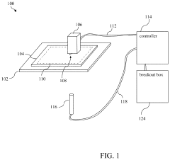
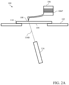
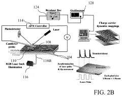
Atomic force microscope based instrumentation for probing nanoscale charge carrier dynamics with improved temporal and spatial resolution
PatentActiveUS20200371135A1
Innovation
- An enhanced AFM system with a conductive tip, an electrically isolated sample holder, a tunable optical source, a function generator, and a bypass circuitry that allows for high bandwidth data collection, enabling the generation of local mobility, carrier lifetime, and impedance maps with nanoscale resolution.
Readout-circuit
PatentPendingUS20250175189A1
Innovation
- A readout-circuit comprising an integrate-and-fire (IAF) circuit and an analog-to-digital converter (ADC) that processes an analog voltage remainder, allowing for the conversion of small analog sensor charges into digital outputs with reduced size, complexity, and noise.


Miniaturization Trends and Integration Possibilities
The miniaturization of Atomic Force Microscopy (AFM) sensing modules represents a significant frontier in advancing portable and integrated measurement systems. Current trends indicate a consistent reduction in the physical dimensions of readout integrated circuits (ICs), with the latest generations achieving footprints below 4mm² while maintaining high performance characteristics. This miniaturization trajectory follows semiconductor industry patterns but with specialized considerations for maintaining signal integrity in increasingly compact designs.
Integration possibilities have expanded dramatically with the emergence of heterogeneous integration techniques. System-in-Package (SiP) approaches now enable the combination of MEMS-based cantilevers with readout ICs in single packages, reducing parasitic capacitances and improving signal-to-noise ratios. The vertical stacking of sensing elements and processing circuitry through 3D integration techniques has demonstrated up to 60% reduction in overall module volume compared to traditional planar implementations.
Advanced packaging technologies, particularly wafer-level packaging (WLP), are enabling hermetic sealing of sensitive components while maintaining minimal form factors. Recent developments in through-silicon via (TSV) technology specifically optimized for AFM applications show promising results for creating ultra-compact sensing modules with improved thermal stability and reduced electromagnetic interference.
Power management innovations are critical enablers of miniaturization, with the latest low-power readout ICs incorporating adaptive biasing schemes that dynamically adjust power consumption based on measurement requirements. Sub-threshold operation techniques have demonstrated functionality with power budgets below 10mW, enabling battery-powered operation for extended periods in portable applications.
The convergence of miniaturization with wireless capabilities presents compelling integration possibilities. Recent prototypes have successfully incorporated Bluetooth Low Energy (BLE) and ultra-wideband (UWB) communication modules alongside AFM readout circuits, enabling wireless data transmission while maintaining compact form factors suitable for in-situ and field applications.
Looking forward, emerging integration approaches utilizing flexible substrates and printed electronics show promise for creating conformable AFM sensing modules that can adapt to non-planar surfaces. Additionally, the integration of machine learning accelerators directly within readout ICs represents an emerging trend, potentially enabling on-device signal processing that reduces data transmission requirements and further decreases system power consumption.
Environmental Impact and Sustainability Considerations
The environmental impact of emerging readout ICs for low-power AFM sensing modules represents a critical consideration in their development and deployment. These advanced integrated circuits, while offering significant performance improvements, must be evaluated through the lens of sustainability across their entire lifecycle. The manufacturing processes for these specialized ICs typically involve energy-intensive cleanroom environments and require rare earth elements and precious metals, raising concerns about resource depletion and extraction impacts.
Energy efficiency stands as a paramount environmental consideration for these readout ICs. The push toward lower power consumption not only extends battery life and improves portability but also significantly reduces the carbon footprint associated with AFM operation. This reduction becomes particularly meaningful when considering the cumulative energy savings across thousands of devices operating continuously in research facilities worldwide.
Material selection and toxicity present another crucial environmental dimension. Many traditional semiconductor manufacturing processes utilize hazardous chemicals including heavy metals, solvents, and etching compounds. Next-generation readout ICs are increasingly designed with environmentally benign alternatives and reduced toxic material content, though challenges remain in maintaining performance while eliminating problematic substances.
End-of-life considerations for these specialized components deserve particular attention. The miniaturization trend in readout ICs complicates recycling efforts, as smaller components with integrated functionalities become more difficult to disassemble and process. Developing effective recovery methods for valuable materials within these ICs represents both an environmental imperative and an economic opportunity.
Regulatory frameworks worldwide are increasingly addressing the environmental aspects of electronic components. Standards such as RoHS (Restriction of Hazardous Substances) and WEEE (Waste Electrical and Electronic Equipment) directives in Europe influence the design parameters for new readout ICs, pushing manufacturers toward more sustainable practices. Companies developing cutting-edge AFM sensing technologies must navigate these evolving requirements while maintaining competitive performance specifications.
The sustainability profile of these components also affects market adoption. Research institutions and industrial users increasingly factor environmental considerations into procurement decisions, creating market incentives for greener technologies. Manufacturers who successfully address sustainability concerns while delivering high-performance, low-power readout ICs gain competitive advantages in this specialized market segment.
Looking forward, emerging design methodologies such as biomimicry and circular economy principles offer promising approaches to further reduce the environmental footprint of these essential components. Innovations in biodegradable substrates and environmentally friendly packaging materials represent frontier areas for sustainability improvements in next-generation AFM sensing modules.
Unlock deeper insights with PatSnap Eureka Quick Research — get a full tech report to explore trends and direct your research. Try now!
Generate Your Research Report Instantly with AI Agent
Supercharge your innovation with PatSnap Eureka AI Agent Platform!