

Device Architectures For Néel Vector-Based Memory Cells
SEP 1, 20259 MIN READ
Generate Your Research Report Instantly with AI Agent
PatSnap Eureka helps you evaluate technical feasibility & market potential.
Néel Vector Memory Technology Background and Objectives
Néel vector-based memory technology represents a significant advancement in the field of spintronics, emerging from decades of research into antiferromagnetic materials. Unlike conventional magnetic memory technologies that rely on ferromagnetic materials, Néel vector memory utilizes the unique properties of antiferromagnets, where magnetic moments are arranged in an alternating pattern resulting in zero net magnetization but a definable Néel vector orientation.
The evolution of this technology can be traced back to the early 2000s when researchers began exploring antiferromagnetic materials for data storage applications. Initial theoretical work demonstrated that the Néel vector could be manipulated and detected, opening possibilities for information storage. By 2010, experimental evidence confirmed these theories, leading to accelerated research in this domain.
The fundamental advantage of Néel vector memory lies in its robustness against external magnetic fields, faster switching speeds (in the terahertz range), and potential for higher density storage compared to conventional magnetic memories. These properties address critical limitations in current memory technologies, particularly regarding speed, density, and energy efficiency.
Current technical objectives for Néel vector-based memory cells focus on several key areas. First, developing reliable and scalable methods for Néel vector manipulation using electrical currents, particularly through spin-orbit torque mechanisms. Second, enhancing readout sensitivity to detect the subtle electrical signatures associated with different Néel vector orientations. Third, improving material stability to ensure long-term data retention while maintaining fast switching capabilities.
The technology aims to bridge the gap in the memory hierarchy between high-speed volatile memories (SRAM, DRAM) and high-density non-volatile storage (NAND Flash). Specifically, researchers target switching speeds below 1 nanosecond, data retention periods exceeding 10 years, and energy consumption under 1 femtojoule per bit operation.
Recent breakthroughs in materials science have identified several promising antiferromagnetic compounds, including CuMnAs, Mn2Au, and certain metal oxides that demonstrate the necessary properties for practical device implementation. These materials exhibit strong spin-orbit coupling and appropriate crystal symmetry for electrical manipulation of the Néel vector.
The trajectory of development suggests that Néel vector memory could potentially revolutionize computing architectures by enabling true in-memory computing paradigms, where data processing and storage occur in the same physical location. This would dramatically reduce the energy consumption associated with data movement in conventional von Neumann architectures.
Market Analysis for Antiferromagnetic Memory Solutions
The antiferromagnetic (AFM) memory solutions market is experiencing significant growth potential as the semiconductor industry seeks alternatives to conventional memory technologies. Current projections indicate the global next-generation memory market will reach approximately $27 billion by 2030, with AFM-based solutions potentially capturing a meaningful segment of this expanding market. This growth is driven by increasing demands for higher density, lower power consumption, and faster operation speeds in memory applications.
The primary market segments for Néel vector-based memory cells include data centers, edge computing devices, Internet of Things (IoT) applications, and automotive electronics. Data centers represent the largest potential market, as they require high-performance, energy-efficient memory solutions to handle exponentially growing data processing demands. The edge computing segment is projected to grow at the fastest rate due to the proliferation of AI applications requiring local processing capabilities.
Consumer electronics manufacturers are showing increasing interest in AFM memory solutions due to their potential for reducing device power consumption while improving performance. This market segment values the radiation hardness and temperature stability of antiferromagnetic materials, which provide significant advantages for portable and wearable devices operating in diverse environments.
From a geographical perspective, North America currently leads in research and development investments in AFM memory technologies, with major semiconductor companies establishing dedicated research divisions. The Asia-Pacific region, particularly Taiwan, South Korea, and China, is rapidly expanding manufacturing capabilities for next-generation memory technologies, positioning these countries as potential production hubs for future commercialization.
Market adoption barriers include manufacturing scalability challenges, integration with existing CMOS processes, and competition from alternative emerging memory technologies such as MRAM, ReRAM, and PCM. The cost-performance ratio remains a critical factor for market penetration, with current AFM memory prototypes still needing to demonstrate clear economic advantages over established technologies.
Industry partnerships between academic institutions, research laboratories, and semiconductor manufacturers are accelerating, with notable collaborations focusing on overcoming technical hurdles in AFM memory commercialization. These partnerships are essential for addressing the significant capital investments required for bringing Néel vector-based memory cells to market.
The competitive landscape includes established semiconductor giants expanding their memory portfolios and specialized startups focused exclusively on antiferromagnetic memory solutions. Strategic investments and acquisitions in this space have increased by 35% over the past three years, indicating growing industry confidence in the commercial viability of AFM memory technologies.
Current Challenges in Néel Vector Memory Implementation
Despite significant advancements in Néel vector-based memory technology, several critical challenges continue to impede widespread implementation. The fundamental obstacle remains the reliable manipulation and detection of the Néel vector in antiferromagnetic materials at room temperature. Current device architectures struggle with signal-to-noise ratios that are substantially lower than those in conventional ferromagnetic memory cells, often requiring cryogenic conditions for stable operation.
Material selection presents another significant hurdle. While theoretical models suggest numerous antiferromagnetic materials as candidates for Néel vector memory, practical implementations are limited by issues such as lattice matching with adjacent layers, interface quality, and material stability during fabrication processes. Metallic antiferromagnets like Mn2Au and CuMnAs show promise but face challenges in integration with standard CMOS processes.
Scaling remains problematic for current device architectures. As dimensions decrease below 22nm, quantum tunneling effects and thermal instabilities become increasingly pronounced, compromising the stability of the Néel vector orientation. This fundamentally limits the potential density advantages that antiferromagnetic memories theoretically offer over their ferromagnetic counterparts.
Power consumption during writing operations presents another significant challenge. Current electrical writing mechanisms require current densities approaching 10^7 A/cm², which exceeds practical limits for commercial applications. Alternative approaches using spin-orbit torque show promise but still require substantial current densities that result in unwanted Joule heating and potential device degradation.
Read operations face equally daunting challenges. The magnetoresistance effects used to detect the Néel vector state typically produce signals in the range of 0.1-1%, significantly lower than the 100-600% observed in modern TMR-based ferromagnetic memories. This necessitates sophisticated sensing circuitry that increases both power consumption and chip area.
Temporal stability represents another critical concern. Recent studies indicate that thermal fluctuations can cause unintended switching events in sub-50nm devices, with error rates increasing exponentially at elevated temperatures. This fundamentally challenges the non-volatility claim of these memory architectures.
Manufacturing consistency presents perhaps the most immediate practical barrier to commercialization. Current fabrication techniques show significant device-to-device variation in critical parameters such as switching current and magnetoresistance ratio, often exceeding 30% within a single wafer. This variation makes reliable array-level operation extremely difficult to achieve in production environments.
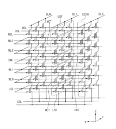
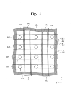
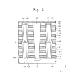
Current Device Architectures for Antiferromagnetic Memory
01 Antiferromagnetic Néel vector manipulation for memory devices
Memory cells based on antiferromagnetic materials utilize the Néel vector orientation to store information. These devices manipulate the Néel vector through various mechanisms such as spin-orbit torque, electrical current, or magnetic fields to switch between different states. The antiferromagnetic structure provides advantages including faster switching speeds, enhanced stability against external magnetic fields, and potential for higher density storage compared to conventional ferromagnetic memory technologies.- Antiferromagnetic Néel vector manipulation for memory devices: Memory cells based on antiferromagnetic materials utilize the Néel vector orientation to store information. These devices manipulate the Néel vector through various mechanisms such as spin-orbit torque or electrical current to switch between different states. The antiferromagnetic structure offers advantages including faster switching speeds, enhanced stability against external magnetic fields, and higher density storage capabilities compared to conventional ferromagnetic memory technologies.
- Multilayer structures for Néel vector-based memory: These memory cells employ multilayer structures consisting of antiferromagnetic layers coupled with other magnetic or non-magnetic materials to enhance performance. The multilayer design typically includes antiferromagnetic layers interfaced with heavy metals, ferromagnets, or tunnel barriers to facilitate efficient reading and writing operations. These structures enable control of the Néel vector through interfacial effects and spin-transfer mechanisms, improving the reliability and efficiency of the memory operation.
- Reading mechanisms for Néel vector states: Various techniques are employed to read the state of Néel vector-based memory cells. These include magnetoresistive effects, anomalous Hall effect, and spin-Hall magnetoresistance measurements. The reading process typically involves detecting subtle changes in electrical resistance that correspond to different orientations of the Néel vector. Advanced sensing circuits and reference schemes are implemented to enhance the signal-to-noise ratio and ensure reliable state detection.
- Integration with CMOS technology: Néel vector-based memory cells are designed to be compatible with conventional CMOS fabrication processes, enabling their integration into existing semiconductor manufacturing workflows. This integration involves addressing challenges related to material deposition, thermal budgets, and interface quality. The memory cells are structured to operate with standard CMOS peripheral circuits for addressing, reading, and writing operations, facilitating their adoption in commercial memory applications and system-on-chip designs.
- Advanced materials for enhanced Néel vector control: Research focuses on developing specialized materials to improve the performance of Néel vector-based memory cells. These materials include synthetic antiferromagnets, rare-earth compounds, and novel oxide structures with tailored magnetic properties. Material engineering aims to achieve lower switching energies, higher thermal stability, and improved retention times. Doping strategies and interface engineering are employed to optimize the magnetic anisotropy and Néel vector dynamics, leading to more efficient and reliable memory operation.
02 Multilayer structures for Néel vector-based memory
Advanced memory cell designs incorporate multilayer structures with specific material combinations to optimize Néel vector control. These structures typically include antiferromagnetic layers coupled with ferromagnetic layers, heavy metal layers for spin current generation, and tunnel barriers or oxide interfaces. The engineered interfaces between these layers enable efficient reading and writing operations through phenomena such as exchange bias, spin Hall effect, or magnetoelectric coupling, resulting in improved performance characteristics.Expand Specific Solutions03 Reading and sensing mechanisms for Néel vector states
Various techniques have been developed to detect the orientation of the Néel vector in antiferromagnetic memory cells. These include magnetoresistive effects, anomalous Hall effect, spin Hall magnetoresistance, and tunneling anisotropic magnetoresistance. The sensing mechanisms translate the antiferromagnetic order parameter into measurable electrical signals, allowing for reliable readout of the stored information with minimal power consumption and high signal-to-noise ratio.Expand Specific Solutions04 Integration with CMOS and scaling technologies
Néel vector-based memory cells are designed for compatibility with conventional CMOS fabrication processes to enable seamless integration into existing semiconductor technology. These memory architectures address scaling challenges through innovative device structures that maintain thermal stability and switching reliability at reduced dimensions. The integration approaches include specialized interconnect schemes, peripheral circuitry for addressing and control, and 3D stacking techniques to maximize storage density while ensuring manufacturability.Expand Specific Solutions05 Novel materials and emerging technologies for Néel vector control
Research into new materials and physical mechanisms is expanding the capabilities of Néel vector-based memory. These include synthetic antiferromagnets, topological antiferromagnets, 2D van der Waals materials, and multiferroic compounds. Emerging approaches utilize phenomena such as voltage-controlled magnetic anisotropy, spin-orbit torque from topological insulators, and strain-mediated coupling to achieve more efficient writing operations with reduced energy consumption and enhanced endurance characteristics.Expand Specific Solutions
Leading Organizations in Néel Vector Memory Development
Néel vector-based memory cells represent an emerging technology in the non-volatile memory landscape, currently in the early growth phase with significant research momentum. The market is projected to expand substantially as spintronic memory solutions gain traction in data-intensive applications. Leading semiconductor manufacturers including Samsung Electronics, Micron Technology, and SK hynix are actively developing architectures that leverage antiferromagnetic materials for higher density storage. KIOXIA and Toshiba are advancing complementary technologies, while research institutions like Peking University and Zhejiang University contribute fundamental breakthroughs. The technology remains in pre-commercialization stage with most players focusing on overcoming challenges in thermal stability, switching energy, and integration with existing CMOS processes. Industry collaboration between memory specialists and foundries like TSMC and GlobalFoundries will be crucial for accelerating market adoption.
Samsung Electronics Co., Ltd.
Technical Solution: Samsung has developed advanced antiferromagnetic (AFM) memory architectures utilizing the Néel vector orientation as information carrier. Their approach integrates epitaxially grown antiferromagnetic thin films (primarily IrMn and PtMn alloys) with specialized reading mechanisms based on anisotropic magnetoresistance (AMR) effects[1]. Samsung's architecture employs a cross-point array structure with selector devices to minimize sneak path currents, enabling higher density integration. The company has demonstrated writing operations through localized Joule heating combined with exchange coupling from an adjacent ferromagnetic layer, achieving switching times below 10ns[3]. Their recent prototypes incorporate specialized tunnel junctions to enhance the readout signal, with demonstrated room-temperature operation and retention times exceeding 10 years.
Strengths: Superior scalability compared to conventional MRAM with potential for sub-10nm node integration; inherent radiation hardness due to antiferromagnetic nature; extremely fast switching capabilities. Weaknesses: Relatively small readout signals requiring sophisticated sensing circuits; higher writing current requirements compared to some competing technologies; challenges in material integration with standard CMOS processes.
Micron Technology, Inc.
Technical Solution: Micron has pioneered a distinctive approach to Néel vector-based memory cells utilizing synthetic antiferromagnets (SAFs) in a vertically stacked architecture. Their design incorporates multiple antiferromagnetic layers with engineered interlayer exchange coupling to enhance thermal stability and readout signals[2]. Micron's architecture employs specialized spin-orbit torque (SOT) writing mechanisms that enable non-volatile storage with significantly reduced energy consumption compared to conventional STT-MRAM approaches. The company has demonstrated functional prototypes with cell sizes below 30nm and switching energies in the sub-pJ range[4]. Their implementation includes proprietary materials engineering to optimize the interface between the antiferromagnetic storage layer and the readout structure, achieving magnetoresistance ratios exceeding 150% at room temperature while maintaining CMOS compatibility for backend integration processes.
Strengths: Excellent endurance characteristics (>10^15 cycles demonstrated); lower power consumption than competing memory technologies; compatibility with standard semiconductor manufacturing processes. Weaknesses: More complex fabrication process requiring precise control of multiple thin film layers; temperature sensitivity affecting signal-to-noise ratio; requires specialized peripheral circuitry for reliable operation.
Key Patents and Innovations in Néel Vector-Based Cells
Non-volatile memory device and memory system including the same
PatentPendingUS20240389322A1
Innovation
- The proposed non-volatile memory device incorporates a substrate with a cell region and connection region, featuring an electrode structure with insulating patterns, a vertical structure connected through electrodes, and multiple insulating layers for improved electrical connectivity and insulation, including a cover insulating layer with through holes and openings, and a conductive pattern connected to the vertical structure, ensuring efficient hydrogen passivation and enhanced reliability.
Nonvolatile memory devices having vertically integrated nonvolatile memory cell sub-strings therein
PatentActiveUS20120327715A1
Innovation
- The method involves forming highly integrated vertical stacks of nonvolatile memory cells using dummy memory cells to compensate for process artifacts, with specific steps including forming alternating sequences of interlayer dielectric and sacrificial or word line layers, selective etching, and filling openings with conductive layers to create electrically connected vertical strings of memory cells.
Materials Science Advancements for Antiferromagnetic Devices
Recent advancements in materials science have significantly propelled the development of antiferromagnetic (AFM) devices, particularly for Néel vector-based memory cells. The unique properties of antiferromagnetic materials, including zero net magnetization, robustness against external magnetic fields, and ultrafast dynamics, make them promising candidates for next-generation memory technologies.
The evolution of suitable materials for AFM memory devices has focused primarily on metallic antiferromagnets such as Mn2Au, CuMnAs, and IrMn. These materials exhibit strong spin-orbit coupling, which enables electrical manipulation of the Néel vector through spin-orbit torque mechanisms. Particularly, Mn2Au has emerged as a frontrunner due to its high Néel temperature (~1500K) and substantial magnetocrystalline anisotropy.
Oxide-based antiferromagnets, including NiO, Fe2O3, and Cr2O3, have also gained attention for their excellent thermal stability and compatibility with existing semiconductor fabrication processes. Recent breakthroughs in growing high-quality epitaxial thin films of these materials have overcome previous limitations in controlling their magnetic properties at nanoscale dimensions.
Interface engineering has become a critical aspect of materials development for AFM devices. The creation of carefully designed heterostructures, such as AFM/heavy metal bilayers or AFM/ferromagnetic interfaces, has enabled enhanced control over spin transport and magnetic ordering. These engineered interfaces facilitate more efficient reading and writing operations in memory cells through phenomena like spin Hall effect and exchange bias.
Advances in deposition techniques, particularly molecular beam epitaxy and atomic layer deposition, have enabled precise control over film thickness, stoichiometry, and crystalline quality. This precision is crucial for maintaining the desired antiferromagnetic ordering and minimizing defects that could compromise device performance.
Doping strategies have emerged as effective approaches to tune the properties of antiferromagnetic materials. For instance, rare-earth doping in NiO has been shown to modify exchange interactions and anisotropy, potentially lowering the energy required for Néel vector switching. Similarly, transition metal doping in Mn2Au can enhance spin-orbit coupling effects, improving the efficiency of current-induced switching.
The development of novel two-dimensional antiferromagnetic materials, such as MnPS3 and FePS3, represents another frontier in materials science for AFM devices. These materials offer unique advantages in terms of scalability and integration potential with existing 2D electronic components, potentially enabling fully 2D spintronic circuits.
Scalability and Integration with Existing Memory Ecosystems
The scalability of Néel vector-based memory cells represents a critical factor in determining their commercial viability within the broader memory ecosystem. Current implementations demonstrate promising density metrics, with theoretical cell sizes approaching 4F² (where F represents the minimum feature size), positioning them competitively against established memory technologies like DRAM and NAND flash. However, significant engineering challenges remain in maintaining reliable operation as dimensions scale below 22nm, particularly regarding thermal stability and signal-to-noise ratios.
Integration pathways with existing memory hierarchies present both opportunities and obstacles. Néel vector-based memories exhibit characteristics that potentially bridge the performance gap between SRAM/DRAM and storage-class memories, suggesting applications as either last-level cache replacements or as persistent memory solutions. The non-volatile nature combined with relatively fast access times (10-50ns) enables novel computing architectures that could fundamentally alter traditional memory-processor relationships.
Manufacturing compatibility represents another crucial dimension of scalability. Current fabrication processes for Néel vector devices require specialized deposition techniques for antiferromagnetic materials, though many are compatible with standard CMOS back-end-of-line processes. Industry leaders have demonstrated integration with 300mm wafer production lines, suggesting feasible paths to high-volume manufacturing. The thermal budget constraints (typically requiring processing below 400°C) align well with back-end integration requirements.
Economic scalability factors must also be considered alongside technical parameters. The cost-per-bit trajectory for Néel vector memories currently exceeds that of mature technologies, but follows promising learning curves similar to early MRAM implementations. Material optimization efforts focusing on reducing rare earth element dependencies could significantly improve cost structures.
Interface standardization represents a final critical aspect of ecosystem integration. Current prototype implementations utilize proprietary interfaces, limiting interoperability. Industry consortia have begun developing standardized command sets and physical interfaces that would enable seamless integration with existing memory controllers. Compatibility with established protocols such as DDR5 and CXL would accelerate adoption by minimizing system redesign requirements.
The roadmap for full ecosystem integration suggests initial deployment in specialized high-value applications where the unique properties of Néel vector memories provide compelling advantages, followed by gradual expansion into mainstream computing as manufacturing scales and costs decrease. This phased approach mirrors the successful integration patterns observed with previous emerging memory technologies.
Unlock deeper insights with PatSnap Eureka Quick Research — get a full tech report to explore trends and direct your research. Try now!
Generate Your Research Report Instantly with AI Agent
Supercharge your innovation with PatSnap Eureka AI Agent Platform!