

Process Integration: Thermal Budgets And Back-End Compatibility
SEP 1, 20259 MIN READ
Generate Your Research Report Instantly with AI Agent
PatSnap Eureka helps you evaluate technical feasibility & market potential.
Thermal Budget Management Evolution and Objectives
Thermal budget management has evolved significantly over the past decades in semiconductor manufacturing, driven by the continuous miniaturization of integrated circuits and the increasing complexity of device structures. In the 1970s and 1980s, thermal budgets were relatively generous, with process temperatures often exceeding 1000°C for extended periods. The primary concern was achieving proper dopant activation and oxide growth, with less emphasis on thermal damage limitations.
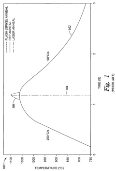
The 1990s marked a pivotal shift as device dimensions shrank below the submicron scale. This era introduced stricter thermal constraints, particularly for shallow junction formation and the prevention of dopant diffusion. The industry began adopting rapid thermal processing (RTP) techniques to minimize the time components spent at elevated temperatures while still achieving necessary thermal effects.
By the early 2000s, the introduction of high-k dielectrics and metal gates further complicated thermal management, as these materials exhibited different thermal sensitivities compared to traditional silicon-based structures. The back-end-of-line (BEOL) processes became increasingly vulnerable to thermal damage, necessitating lower processing temperatures, typically below 450°C.
The current decade has witnessed the emergence of three-dimensional architectures such as FinFETs and gate-all-around structures, imposing even more stringent thermal budget constraints. Advanced packaging technologies like 3D integration and heterogeneous integration have further complicated thermal management, requiring precise control to prevent damage to previously fabricated layers and interfaces.
Today's thermal budget objectives focus on several critical aspects. First, maintaining the integrity of temperature-sensitive materials, particularly in advanced node technologies where thermal stability windows have narrowed significantly. Second, ensuring compatibility between front-end and back-end processes, where thermal requirements often conflict. Third, optimizing thermal cycles to achieve desired material transformations while minimizing unintended effects like dopant diffusion or interface degradation.
Looking forward, the industry aims to develop more precise thermal management techniques that can deliver highly localized heating, potentially through advanced laser annealing or microwave processing. Another objective is the creation of comprehensive thermal models that can predict cumulative thermal effects across multiple process steps, enabling more efficient process integration. Additionally, there is growing interest in low-temperature alternatives for traditionally high-temperature processes, such as atomic layer deposition and plasma-enhanced techniques.
The ultimate goal remains balancing the thermal requirements for optimal device performance with the increasingly restrictive thermal constraints imposed by advanced materials and architectures, particularly in the context of back-end compatibility.
Market Demand for Advanced Process Integration Solutions
The semiconductor industry's demand for advanced process integration solutions has been growing exponentially, driven by the continuous miniaturization of electronic devices and the increasing complexity of integrated circuits. Market research indicates that the global semiconductor process control equipment market is projected to reach $9.2 billion by 2026, with a compound annual growth rate of 6.3% from 2021. This growth is primarily fueled by the need for more sophisticated thermal budget management and back-end compatibility solutions.
Consumer electronics manufacturers are particularly vocal about their requirements for process integration technologies that can support the development of smaller, more powerful devices with extended battery life. The smartphone market, valued at approximately $448 billion in 2023, continues to push for advanced semiconductor processes that can accommodate higher transistor densities while maintaining thermal stability during manufacturing.
Data center operators represent another significant market segment demanding improved process integration solutions. With the global data center market expected to reach $288 billion by 2027, these facilities require semiconductors that can handle increased computational loads while minimizing heat generation. This has created substantial demand for thermal budget optimization techniques that ensure reliable performance under high-stress conditions.
The automotive industry has emerged as a rapidly growing consumer of advanced semiconductor technologies, especially with the rise of electric vehicles and autonomous driving systems. Market analysts estimate that semiconductor content per vehicle will increase from $475 in 2020 to over $1,600 by 2030. Automotive-grade chips require exceptional reliability and must withstand harsh operating environments, creating unique challenges for process integration and thermal management.
IoT device manufacturers represent yet another expanding market segment, with projections indicating over 75 billion connected devices worldwide by 2025. These devices often operate in resource-constrained environments, creating demand for semiconductor processes that can balance performance with power efficiency through optimized thermal budgets.
Geographically, Asia-Pacific dominates the market demand, accounting for approximately 60% of global semiconductor manufacturing capacity. North America follows with strong demand driven by data center expansion and defense applications, while Europe shows growing interest particularly in automotive and industrial semiconductor applications requiring advanced process integration solutions.
Current Challenges in Back-End Thermal Compatibility
The integration of advanced semiconductor processes faces significant thermal compatibility challenges in back-end-of-line (BEOL) operations. Current manufacturing technologies encounter thermal budget constraints that severely limit process options and material selections. The maximum allowable temperature for BEOL processes has steadily decreased from approximately 450°C for older technology nodes to below 400°C for advanced nodes, with some critical steps requiring temperatures as low as 300-350°C to prevent damage to underlying structures.
A primary challenge is the thermal degradation of metal interconnects, particularly copper and aluminum. At elevated temperatures, these metals can diffuse into surrounding dielectric materials, creating reliability issues such as increased leakage currents and potential short circuits. Additionally, thermal cycling induces mechanical stress due to coefficient of thermal expansion (CTE) mismatches between different materials, leading to delamination, cracking, and void formation in interconnect structures.
Low-k dielectric materials, essential for reducing RC delays in advanced nodes, present another significant thermal compatibility issue. These materials are particularly vulnerable to thermal degradation, with many organic low-k materials beginning to decompose at temperatures above 350-400°C. This decomposition can lead to increased dielectric constants, negating their intended benefits, and compromising structural integrity.
The integration of memory elements in logic processes introduces additional thermal constraints. For instance, MRAM (Magnetic Random Access Memory) fabrication requires precise control of magnetic layer properties that can be irreversibly altered at temperatures exceeding 400°C. Similarly, phase-change memory materials have specific crystallization temperature requirements that must be maintained within narrow windows.
3D integration and advanced packaging technologies compound these challenges. Through-silicon vias (TSVs) and micro-bumps used in 3D stacking create complex thermal management requirements. The sequential processing of multiple layers means that each subsequent process must operate at progressively lower temperatures to avoid damaging previously fabricated structures.
Current workarounds include developing specialized low-temperature deposition techniques such as atomic layer deposition (ALD) and plasma-enhanced chemical vapor deposition (PECVD) that can operate effectively below 350°C. However, these processes often result in films with inferior quality compared to their higher-temperature counterparts, creating trade-offs between thermal compatibility and device performance.
The semiconductor industry is actively researching alternative approaches such as selective laser annealing and microwave processing that can provide localized heating without affecting surrounding structures. However, these techniques face challenges in uniformity, throughput, and integration with existing manufacturing flows, limiting their widespread adoption in high-volume manufacturing environments.
Mainstream Thermal Budget Management Approaches
01 Thermal budget management in semiconductor manufacturing
Thermal budget management is critical in semiconductor manufacturing processes to control the heat exposure of wafers. This involves optimizing temperature profiles, process durations, and heat distribution to prevent damage to semiconductor structures while ensuring proper formation of device features. Effective thermal budget management improves device performance, reliability, and manufacturing yield by minimizing thermal stress and unwanted diffusion of dopants.- Thermal budget management in semiconductor manufacturing: Thermal budget management is critical in semiconductor manufacturing processes to control the heat exposure of wafers during fabrication. This involves optimizing temperature profiles, process durations, and heat distribution to prevent damage to semiconductor structures while ensuring proper formation of device features. Effective thermal budget management improves device performance, reliability, and manufacturing yield.
- Integration of thermal processes in semiconductor fabrication: Process integration techniques combine multiple thermal steps to reduce the overall thermal budget while maintaining manufacturing efficiency. This includes sequencing high and low-temperature processes strategically, combining compatible thermal steps, and implementing rapid thermal processing methods. Such integration minimizes thermal stress on semiconductor materials and structures while optimizing production throughput.
- Thermal budget optimization in manufacturing systems: Manufacturing systems employ sophisticated algorithms and control systems to optimize thermal budgets across production lines. These systems monitor and adjust thermal parameters in real-time, schedule processes to balance thermal loads, and implement predictive models to anticipate thermal requirements. Advanced thermal budget optimization improves energy efficiency, reduces production costs, and enhances product quality.
- Energy management in thermal processing equipment: Energy management strategies for thermal processing equipment focus on reducing power consumption while maintaining process integrity. This includes implementing energy-efficient heating technologies, thermal insulation improvements, heat recovery systems, and intelligent power management. These approaches help minimize the environmental impact of manufacturing operations while optimizing thermal budget utilization.
- Advanced materials and structures for thermal budget reduction: Novel materials and structural designs are developed to function effectively under reduced thermal budgets. These include low-temperature compatible materials, thermally resilient structures, and advanced thin film technologies. By employing materials that can be processed at lower temperatures or withstand thermal cycling better, manufacturers can significantly reduce the overall thermal budget requirements while maintaining or improving device performance.
02 Integration of thermal processes in semiconductor fabrication
Process integration involves coordinating multiple thermal steps in semiconductor fabrication to optimize the overall thermal budget. This includes sequencing high and low-temperature processes, combining compatible thermal steps, and implementing rapid thermal processing techniques. Strategic integration of thermal processes helps maintain the integrity of previously formed structures while enabling subsequent processing steps, ultimately leading to more efficient manufacturing workflows.Expand Specific Solutions03 Thermal budget monitoring and control systems
Advanced monitoring and control systems are employed to track and manage thermal budgets in semiconductor manufacturing. These systems utilize real-time temperature sensors, predictive modeling, and feedback control mechanisms to ensure precise thermal management. By continuously monitoring process conditions and making adjustments as needed, these systems help maintain consistent quality and prevent thermal budget violations that could compromise device performance.Expand Specific Solutions04 Low thermal budget processing techniques
Low thermal budget processing techniques are developed to minimize heat exposure while achieving desired material transformations. These include laser annealing, microwave processing, flash lamp annealing, and low-temperature deposition methods. Such techniques enable the fabrication of advanced semiconductor devices with thermally sensitive materials and ultra-shallow junctions by providing precise, localized heating while keeping the overall thermal budget low.Expand Specific Solutions05 Thermal budget optimization for advanced device manufacturing
Optimization strategies for thermal budgets in advanced device manufacturing involve computational modeling, design of experiments, and machine learning techniques. These approaches help identify the minimum thermal requirements for each process step while maintaining device quality. Thermal budget optimization becomes increasingly important as device dimensions shrink and new materials are introduced, requiring careful balancing of competing thermal requirements across the entire manufacturing process.Expand Specific Solutions
Leading Semiconductor Process Integration Companies
Process Integration: Thermal Budgets and Back-End Compatibility is currently in a growth phase, with the global semiconductor thermal management market expanding at a CAGR of approximately 8-9%. The market size is projected to reach $12-15 billion by 2027, driven by increasing chip complexity and miniaturization demands. Technologically, the field is moderately mature but evolving rapidly as companies address thermal challenges in advanced nodes. Intel leads with comprehensive thermal management solutions across their manufacturing processes, while Applied Materials and Samsung Electronics offer specialized equipment and integration techniques. ASM IP Holding and TSMC have made significant advancements in low-thermal budget processes, with emerging players like MediaTek and Axcelis Technologies developing niche solutions for specific thermal integration challenges.
Intel Corp.
Technical Solution: Intel has developed a comprehensive thermal budget management system for their advanced node processes, particularly for their 3D stacking technologies like Foveros. Their approach includes selective deposition techniques that enable low-temperature processing (below 500°C) for back-end-of-line (BEOL) compatibility. Intel's SuperFin technology incorporates enhanced power delivery networks with reduced resistance, allowing for better thermal dissipation across the chip. They've also pioneered hybrid bonding techniques that maintain thermal integrity while enabling heterogeneous integration. Intel's process uses precision-controlled rapid thermal annealing (RTA) systems that minimize thermal exposure while ensuring proper dopant activation and defect healing in their transistor structures.
Strengths: Proprietary thermal simulation tools provide accurate modeling for complex 3D structures; extensive manufacturing experience enables practical implementation of theoretical approaches. Weaknesses: Solutions are often optimized for their specific process nodes and may not be universally applicable; high implementation costs limit accessibility for smaller manufacturers.
Applied Materials, Inc.
Technical Solution: Applied Materials has developed the Endura® Clover™ MRAM PVD platform specifically designed to address thermal budget challenges in advanced semiconductor manufacturing. This system enables precise deposition of magnetic tunnel junction (MTJ) layers at controlled temperatures to maintain BEOL compatibility. Their Producer® GT™ PECVD system incorporates advanced temperature management for low-temperature dielectric deposition, critical for maintaining thermal budgets. Applied Materials also offers the Producer® Precision® CVD system that utilizes pulsed plasma deposition techniques to achieve high-quality films at reduced thermal loads. Their integrated approach combines materials engineering with process control to enable manufacturers to implement thermal budget-conscious solutions across multiple process steps.
Strengths: Comprehensive equipment portfolio addresses thermal challenges across multiple process steps; strong materials science expertise enables novel solutions to thermal constraints. Weaknesses: Solutions require significant capital investment; integration with existing fab equipment from other vendors can present compatibility challenges.
Key Innovations in Low-Temperature Processing
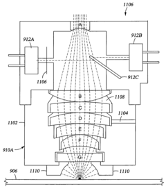
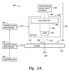
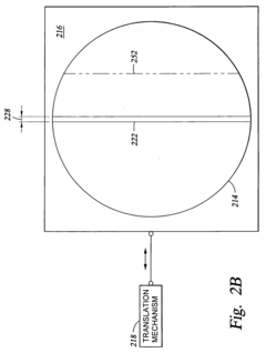
Scanning laser light source
PatentInactiveUS20070114214A1
Innovation
- A method and apparatus utilizing a continuous wave electromagnetic radiation source focused into a line, which is translated across the substrate surface to provide high ramp rates and localized heating, ensuring homogenous thermal exposure and reducing thermal budget by only heating the substrate surface, thereby allowing for rapid heating and cooling without exposing the bulk substrate to extreme temperatures.
Thermal FLUX processing by scanning electromagnetic radiation
PatentInactiveEP1507625A1
Innovation
- A method and apparatus that uses a continuous wave electromagnetic radiation source focused into a line, translated across the substrate surface to achieve high ramp rates and homogenous thermal exposure, allowing for localized heating and rapid temperature changes without heating the entire substrate, thereby reducing thermal budget and minimizing pattern dependencies.
Material Science Advancements for Back-End Processing
Recent advancements in material science have significantly transformed back-end processing capabilities, addressing the critical challenges of thermal budgets and process integration. Novel low-temperature materials have emerged as key enablers for advanced semiconductor manufacturing, particularly for 3D integration and heterogeneous packaging technologies where thermal constraints are paramount.
The development of low-k dielectric materials with improved thermal stability has been crucial for maintaining signal integrity while reducing RC delays in interconnect structures. These materials can now withstand back-end processing temperatures without degradation of their electrical properties, enabling more reliable multi-layer metallization schemes. Simultaneously, research into alternative barrier and liner materials has yielded options that can be deposited at lower temperatures while maintaining excellent adhesion and diffusion prevention properties.
Metal alloys specifically engineered for back-end compatibility represent another significant advancement. These alloys offer lower resistivity than traditional options while requiring reduced thermal budgets for deposition and annealing. Copper-manganese and copper-aluminum systems, for instance, demonstrate superior electromigration resistance without necessitating high-temperature processing steps that would damage underlying structures.
Self-forming barrier technologies have emerged as a promising approach, where the barrier layer forms in-situ during the initial stages of metallization. This process occurs at significantly lower temperatures than conventional barrier deposition methods, preserving the integrity of temperature-sensitive components while ensuring reliable interconnect performance.
Atomic layer deposition (ALD) techniques have been refined to enable conformal coating of high-aspect-ratio structures at temperatures below 300°C, addressing one of the most challenging aspects of back-end processing. These techniques allow for precise control of film thickness and composition, critical for increasingly complex 3D architectures where traditional deposition methods struggle to provide adequate coverage.
Polymer-based temporary bonding materials represent another important advancement, facilitating wafer thinning and 3D stacking processes while maintaining thermal stability throughout subsequent processing steps. These materials can be applied and removed at low temperatures, enabling sophisticated heterogeneous integration schemes without compromising device performance.
The collective impact of these material science advancements has been transformative, enabling more complex integration schemes while respecting the thermal constraints inherent to back-end processing. As device architectures continue to evolve toward greater three-dimensionality and heterogeneous integration, these materials innovations will remain central to overcoming the fundamental challenges of thermal budgets in advanced semiconductor manufacturing.
Economic Impact of Thermal Budget Optimization
The optimization of thermal budgets in semiconductor manufacturing processes represents a significant economic lever that extends far beyond mere technical considerations. When properly managed, thermal budget optimization directly impacts manufacturing costs through reduced energy consumption, which can account for 5-15% of total operational expenses in semiconductor fabrication facilities.
Thermal budget optimization also substantially affects production throughput and yield rates. Advanced thermal management techniques have demonstrated the potential to increase wafer throughput by 8-12% while simultaneously reducing defect rates by up to 20% in back-end processes. These improvements translate directly to higher profit margins and enhanced return on investment for manufacturing facilities.
Equipment lifecycle and maintenance costs represent another critical economic dimension. Excessive thermal stress accelerates equipment degradation, leading to more frequent maintenance cycles and premature replacement of capital-intensive tools. Studies indicate that optimized thermal profiles can extend equipment service life by 15-30%, representing millions in deferred capital expenditures for large-scale operations.
From a competitive standpoint, manufacturers with superior thermal budget management capabilities gain significant market advantages. The ability to process temperature-sensitive materials enables the development of differentiated products with enhanced performance characteristics, potentially commanding premium pricing in specialized market segments such as high-performance computing and advanced mobile applications.
Time-to-market acceleration represents perhaps the most strategic economic benefit. Optimized thermal processes that maintain back-end compatibility allow for faster integration of new materials and device architectures into existing production lines. This capability can reduce development cycles by 3-6 months, providing first-mover advantages in rapidly evolving semiconductor markets.
The economic implications extend to supply chain resilience as well. Facilities with flexible thermal processing capabilities can more readily adapt to material supply disruptions by accommodating alternative materials with different thermal requirements, reducing production vulnerabilities in uncertain global supply environments.
Finally, regulatory compliance and sustainability objectives increasingly influence economic calculations. Enhanced thermal efficiency contributes to reduced carbon footprints, potentially qualifying manufacturers for carbon credits or preferential treatment under emerging environmental regulations, while simultaneously reducing exposure to future carbon taxation schemes.
Unlock deeper insights with PatSnap Eureka Quick Research — get a full tech report to explore trends and direct your research. Try now!
Generate Your Research Report Instantly with AI Agent
Supercharge your innovation with PatSnap Eureka AI Agent Platform!