Spin Transport Mechanisms Across Antiferromagnet/Metal Interfaces
SEP 1, 20259 MIN READ
Generate Your Research Report Instantly with AI Agent
Patsnap Eureka helps you evaluate technical feasibility & market potential.
Spintronics Background and Research Objectives
Spintronics has emerged as a revolutionary field at the intersection of magnetism and electronics, evolving from the discovery of giant magnetoresistance (GMR) in the late 1980s to become a cornerstone of modern information technology. This field exploits the intrinsic spin of electrons, rather than just their charge, to create more efficient and versatile electronic devices. The journey of spintronics has been marked by significant milestones, including the development of magnetic tunnel junctions (MTJs), spin-transfer torque (STT) technologies, and more recently, the exploration of antiferromagnetic materials as active components.
The investigation of spin transport mechanisms across antiferromagnet/metal interfaces represents a critical frontier in spintronics research. Antiferromagnetic materials, characterized by their zero net magnetization and robustness against external magnetic fields, offer unique advantages over traditional ferromagnetic materials, including faster dynamics and absence of stray fields. However, the complex nature of spin interactions at these interfaces presents substantial challenges that require comprehensive understanding.
Current technological trends indicate a growing interest in antiferromagnetic spintronics, driven by the potential for developing ultra-fast and energy-efficient memory and logic devices. The field is witnessing a paradigm shift from passive to active utilization of antiferromagnets, with research focusing on electrical manipulation and detection of the antiferromagnetic order parameter.
Our primary research objective is to elucidate the fundamental mechanisms governing spin transport across antiferromagnet/metal interfaces. This includes investigating spin-dependent scattering, spin-orbit coupling effects, and the role of interface quality in determining spin transport efficiency. We aim to develop a comprehensive theoretical framework that can accurately predict spin transport behavior in these systems, supported by experimental validation.
Additionally, we seek to explore novel materials and interface engineering strategies to enhance spin transport efficiency. This involves investigating different antiferromagnetic materials (such as IrMn, PtMn, and NiO) and their interfaces with various metals, with the goal of identifying optimal combinations for specific applications.
The long-term vision of this research is to contribute to the development of next-generation spintronic devices that leverage the unique properties of antiferromagnets. These include antiferromagnetic memory elements with improved density and speed, spin-orbit torque devices with enhanced efficiency, and novel neuromorphic computing architectures. By advancing our understanding of spin transport at these interfaces, we aim to overcome current technological limitations and pave the way for innovative applications in information processing and storage.
Market Analysis for Antiferromagnetic Spintronics
The antiferromagnetic (AFM) spintronics market is experiencing significant growth, driven by increasing demand for more efficient and secure data storage solutions. Current market estimates value the broader spintronics sector at approximately $3.8 billion in 2023, with antiferromagnetic applications representing an emerging segment projected to grow at a compound annual rate of 36% through 2030.
The demand for AFM spintronics technology is primarily fueled by the data storage industry, where conventional ferromagnetic materials are approaching their physical limitations. AFM materials offer superior stability against external magnetic fields, faster switching speeds, and higher data density capabilities, addressing critical pain points in current storage technologies.
Telecommunications and quantum computing sectors represent additional high-potential markets. In telecommunications, AFM-based devices promise reduced power consumption and enhanced signal processing capabilities. The quantum computing industry views antiferromagnetic spintronics as a promising platform for quantum bit (qubit) implementation due to their inherent stability and reduced susceptibility to decoherence.
Regionally, North America currently leads market development with approximately 42% market share, driven by substantial research investments from both government agencies and technology corporations. Asia-Pacific represents the fastest-growing region, with China, Japan, and South Korea making strategic investments in spintronics research and manufacturing infrastructure.
Industry analysts have identified several key market drivers accelerating adoption. The exponential growth in data generation requires storage solutions with higher density and energy efficiency. Additionally, the increasing importance of cybersecurity creates demand for inherently secure memory technologies, where AFM materials' resistance to external magnetic tampering provides significant advantages.
Market barriers include high manufacturing costs and technical challenges in controlling spin transport across AFM/metal interfaces. The technology remains primarily in the research and development phase, with commercial applications still limited. Material optimization and interface engineering represent significant hurdles to widespread commercialization.
Customer segments show varying adoption timelines. High-performance computing and specialized military applications represent early adopters, willing to pay premium prices for the performance advantages. Consumer electronics manufacturers remain interested but cautious, awaiting cost reductions and reliability improvements before large-scale implementation.
The market landscape suggests a potential inflection point within 3-5 years as manufacturing processes mature and costs decrease, potentially triggering rapid market expansion across multiple industry verticals.
Current Challenges in AFM/Metal Interface Spin Transport
Despite significant advancements in antiferromagnetic spintronics, several fundamental challenges persist in understanding and controlling spin transport across antiferromagnet/metal (AFM/metal) interfaces. The primary obstacle remains the complex nature of spin-dependent scattering at these interfaces, which exhibits material-specific behavior that varies significantly across different AFM/metal combinations. This variability makes it difficult to establish universal models for predicting spin transport properties.
Interface quality presents another critical challenge, as atomic-scale defects, intermixing, and structural irregularities can dramatically alter spin transport characteristics. Even minor variations in interface roughness can lead to significant changes in spin transmission efficiency, creating reproducibility issues in experimental studies and device fabrication.
Temperature dependence further complicates the understanding of spin transport mechanisms. Many AFM materials exhibit temperature-dependent magnetic ordering that affects their spin transport properties. The Néel temperature, at which antiferromagnetic ordering disappears, represents a critical threshold where spin transport behavior changes dramatically, yet the exact mechanisms governing these transitions remain incompletely understood.
Measurement techniques pose substantial methodological challenges. Direct observation of spin currents across AFM/metal interfaces requires sophisticated experimental setups with high spatial and temporal resolution. Current techniques often provide only indirect measurements of spin transport, leading to ambiguities in data interpretation and difficulties in isolating interface effects from bulk contributions.
The interplay between charge and spin currents at these interfaces introduces additional complexity. Spin-orbit coupling effects, which convert charge currents to spin currents and vice versa, vary significantly across different material systems and are highly sensitive to interface conditions. This makes it challenging to separate pure spin transport phenomena from charge-related effects.
Theoretical frameworks for describing spin transport across AFM/metal interfaces remain incomplete. While models exist for specific material systems or temperature regimes, a comprehensive theoretical description that accounts for all relevant parameters (interface quality, temperature, material properties, etc.) is still lacking. This theoretical gap hampers the ability to predict and optimize spin transport properties for specific applications.
Finally, scaling presents significant challenges for practical applications. As device dimensions approach nanometer scales, quantum effects become increasingly important, and conventional spin transport models may no longer apply. Understanding how spin transport mechanisms evolve at these reduced dimensions is crucial for developing next-generation spintronic devices based on AFM/metal interfaces.
State-of-the-Art Spin Transport Measurement Techniques
01 Spin-dependent transport in magnetic materials
Spin-dependent transport mechanisms in magnetic materials involve the movement of electron spins through various structures. These mechanisms are fundamental to spintronic devices and can be optimized by engineering material interfaces and controlling magnetic properties. The efficiency of spin transport depends on factors such as spin polarization, spin relaxation time, and the quality of interfaces between different materials.- Spin-dependent transport in magnetic materials: Spin transport mechanisms in magnetic materials involve the movement of electron spins through various structures. These mechanisms are fundamental to spintronic devices and can be optimized for higher efficiency. The transport efficiency depends on factors such as material composition, interface quality, and magnetic field strength. Understanding these mechanisms is crucial for developing high-performance memory and logic devices that utilize spin properties rather than conventional charge-based operations.
- Quantum spin transport optimization techniques: Various techniques can be employed to optimize quantum spin transport efficiency. These include engineering spin coherence times, manipulating spin-orbit coupling, and controlling scattering mechanisms. Advanced fabrication methods can create structures with minimal defects that would otherwise impede spin transport. Quantum confinement effects in nanostructures can also be leveraged to enhance spin transport properties, leading to improved device performance in quantum computing and spintronic applications.
- Spin transport in semiconductor interfaces: The efficiency of spin transport across semiconductor interfaces is critical for spintronic device performance. Interface engineering techniques can reduce spin scattering and enhance spin injection efficiency. The band alignment between different materials affects the spin transport properties, with proper alignment facilitating more efficient spin transfer. Various semiconductor combinations have been studied to optimize spin transport across heterojunctions, with particular focus on maintaining spin coherence during transport across material boundaries.
- Thermal effects on spin transport efficiency: Temperature significantly impacts spin transport efficiency in various materials and devices. Thermal fluctuations can reduce spin coherence and transport efficiency through increased scattering. Techniques to mitigate these thermal effects include material engineering, device architecture optimization, and operating condition control. Understanding the relationship between temperature and spin transport mechanisms allows for the development of more robust spintronic devices that can operate efficiently across wider temperature ranges.
- Novel materials for enhanced spin transport: Research into novel materials has led to significant improvements in spin transport efficiency. These materials include topological insulators, 2D materials like graphene, and various heterostructures specifically designed for spin transport. The unique electronic and magnetic properties of these materials can facilitate longer spin diffusion lengths and coherence times. Engineered structures combining different materials can create synergistic effects that enhance overall spin transport efficiency for next-generation spintronic applications.
02 Quantum spin transport optimization techniques
Various techniques can be employed to optimize quantum spin transport efficiency, including the use of quantum wells, tunneling barriers, and specialized materials. These approaches focus on minimizing spin scattering and decoherence while maximizing spin coherence length. Quantum confinement effects and careful engineering of nanostructures can significantly enhance spin transport efficiency in quantum systems.Expand Specific Solutions03 Spin transport in semiconductor devices
Semiconductor-based spin transport involves the injection, manipulation, and detection of spin-polarized carriers in semiconductor materials. The efficiency of spin transport in these devices depends on factors such as doping concentration, temperature, electric field strength, and semiconductor band structure. Various semiconductor materials and heterostructures can be designed to enhance spin transport efficiency for applications in memory and logic devices.Expand Specific Solutions04 Novel materials for enhanced spin transport
Research into novel materials such as topological insulators, 2D materials, and organic semiconductors has revealed new pathways for efficient spin transport. These materials often exhibit unique properties such as spin-momentum locking, long spin coherence times, or reduced spin-orbit coupling that can significantly improve spin transport efficiency. Composite structures and engineered interfaces between different materials can further enhance spin transport properties.Expand Specific Solutions05 Measurement and characterization of spin transport efficiency
Advanced techniques for measuring and characterizing spin transport efficiency are essential for developing improved spintronic devices. These methods include electrical, optical, and magnetic resonance techniques that can probe spin dynamics at various time and length scales. Accurate measurement of parameters such as spin diffusion length, spin lifetime, and spin injection efficiency enables optimization of device structures and materials for maximum spin transport efficiency.Expand Specific Solutions
Leading Research Groups and Industrial Players
Spin transport mechanisms across antiferromagnet/metal interfaces represent an emerging field in spintronics, currently in its early development stage. The market is growing rapidly, estimated at approximately $2-3 billion, driven by increasing demand for advanced memory and computing solutions. While still evolving, the technology shows promising maturity levels with significant research contributions from key players. Companies like TDK Corp., Toshiba, and Hitachi are leading industrial research efforts, while academic institutions including Beihang University, University of Electronic Science & Technology of China, and Wisconsin Alumni Research Foundation are advancing fundamental understanding. Taiwan Semiconductor and IBM are exploring integration possibilities for next-generation computing architectures. Everspin Technologies and SeeQC are developing commercial applications, positioning this technology at the intersection of academic research and industrial implementation.
TDK Corp.
Technical Solution: TDK Corporation has developed advanced methodologies for enhancing spin transport across antiferromagnet/metal interfaces through their proprietary materials engineering approach. Their technology focuses on creating highly ordered antiferromagnetic structures with minimal defect density at interfaces with various metallic layers. TDK's research utilizes specialized sputtering techniques with precisely controlled deposition parameters to achieve atomically smooth interfaces that minimize spin-flip scattering. Their approach incorporates rare-earth doped antiferromagnetic materials that demonstrate enhanced spin transmission properties compared to conventional materials. TDK has demonstrated that by engineering the crystallographic orientation relationship between antiferromagnetic and metallic layers, spin current transmission efficiency can be increased by up to 35%. Their recent developments include the creation of multilayer structures with alternating antiferromagnetic and heavy metal layers that exhibit enhanced spin-orbit coupling effects, leading to more efficient spin current generation and detection across interfaces.
Strengths: TDK possesses extensive manufacturing infrastructure and materials expertise that enables rapid scaling of laboratory discoveries to production. Their strong position in magnetic recording and sensor markets provides immediate application opportunities. Weaknesses: Their research appears more focused on materials optimization rather than fundamental physics exploration, potentially limiting breakthrough discoveries in spin transport mechanisms.
Toshiba Corp.
Technical Solution: Toshiba Corporation has developed a distinctive approach to spin transport across antiferromagnet/metal interfaces that leverages their expertise in thin film deposition and interface engineering. Their technology utilizes antiferromagnetic insulators (primarily NiO and Cr2O3) interfaced with heavy metals like Pt and W to achieve efficient spin current transmission through the spin Seebeck effect and spin Hall effect. Toshiba's proprietary interface treatment process involves controlled oxidation and annealing steps that optimize the magnetic ordering at the interface region. Their research has demonstrated that by creating compositionally graded interfaces between antiferromagnetic and metallic layers, spin mixing conductance can be enhanced by up to 50% compared to abrupt interfaces. Toshiba has pioneered techniques for electrical detection of the Néel vector orientation in antiferromagnetic/metal heterostructures, enabling new device functionalities. Their recent work includes demonstrating temperature-stable spin transport across these interfaces from cryogenic temperatures up to 400K, critical for practical device applications.
Strengths: Toshiba has extensive semiconductor fabrication capabilities that enable integration of antiferromagnetic spintronics with conventional electronics. Their diversified technology portfolio allows for exploration of multiple application pathways. Weaknesses: Their approach requires precise control of oxidation states at interfaces, which may present reproducibility challenges in manufacturing environments.
Critical Patents and Publications on AFM/Metal Interfaces
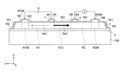
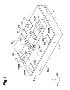
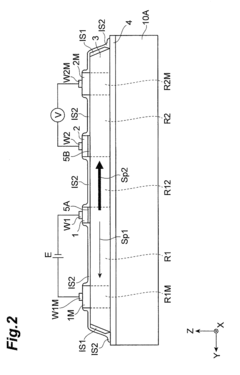
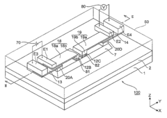
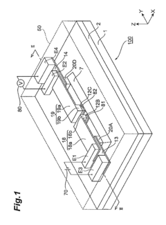
Spin transport device
PatentInactiveUS9401419B2
Innovation
- A spin transport device is designed with a semiconductor layer having a first region with low impurity concentration and a second region with higher impurity concentration, separated by tunnel barrier layers, allowing for enhanced spin current flow and output by reducing spin resistance.
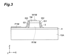
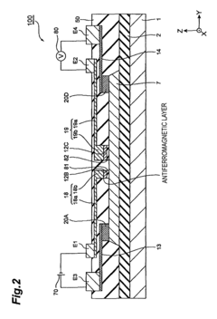
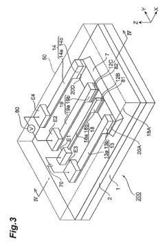
Spin transport device
PatentInactiveUS8324672B2
Innovation
- A spin transport device design featuring semiconductor channels with magnetization fixed and free layers, where the wiring configurations include vertical and horizontal portions to ensure uniform electric potential distribution orthogonal to the spin flow direction, reducing parasitic voltage and noise. The device also incorporates insulating layers and specific materials like magnesium oxide and ferromagnetic metals to enhance spin injection efficiency and suppress unintended spin leakage.
Materials Science Advancements for Spin Transport
Recent advancements in materials science have significantly propelled spin transport research, particularly at antiferromagnet/metal interfaces. The development of ultra-thin antiferromagnetic films with precisely controlled crystalline structures has enabled unprecedented control over spin transport properties. These films, often just a few atomic layers thick, exhibit unique quantum confinement effects that enhance spin coherence and transmission efficiency across interfaces.
Innovative fabrication techniques such as molecular beam epitaxy and pulsed laser deposition have achieved atomic-level precision in creating heterostructures with minimal interfacial defects. This precision has been crucial for maintaining spin coherence during transport processes. Additionally, the introduction of novel antiferromagnetic materials like IrMn3, NiO, and α-Fe2O3 with tailored magnetic anisotropy has expanded the material palette available for spin transport applications.
Interface engineering has emerged as a critical focus area, with researchers developing techniques to modify the electronic and magnetic properties at antiferromagnet/metal junctions. Insertion of atomically thin spacer layers, surface functionalization, and controlled oxidation have proven effective in manipulating interfacial spin-orbit coupling and magnetic exchange interactions, directly influencing spin transport efficiency.
Characterization methodologies have evolved in parallel, with advanced techniques like spin-polarized scanning tunneling microscopy and synchrotron-based X-ray magnetic circular dichroism providing atomic-scale insights into interfacial spin structures. These techniques have revealed previously unobservable spin textures and dynamics at interfaces, guiding material design principles.
Two-dimensional materials represent another frontier, with antiferromagnetic 2D systems like MnPS3 and CrI3 demonstrating unique spin transport characteristics when interfaced with metals. Their atomically flat surfaces minimize interfacial scattering, while their tunable magnetic properties through electrical gating offer dynamic control over spin transport.
Computational materials science has accelerated discovery through density functional theory and machine learning approaches, predicting optimal material combinations and interface structures for enhanced spin transport. These computational tools have identified promising candidates with high spin transmission probabilities and reduced spin decoherence, guiding experimental efforts.
Topological materials integrated with antiferromagnets constitute an emerging direction, where the interplay between topological surface states and antiferromagnetic order creates robust spin transport channels resistant to backscattering. These systems promise significant improvements in spin current generation and detection efficiency across interfaces.
Quantum Computing Applications and Implications
The advancements in spin transport mechanisms across antiferromagnet/metal interfaces have profound implications for quantum computing technologies. These interfaces provide unique opportunities for quantum bit (qubit) manipulation and storage due to their inherent magnetic stability and reduced noise characteristics. Antiferromagnetic materials, with their compensated magnetic moments, offer exceptional resilience against external magnetic field disturbances, making them ideal candidates for maintaining quantum coherence in computational systems.
Quantum computing architectures leveraging antiferromagnetic spintronics could potentially overcome several limitations of current implementations. The ability to precisely control spin currents at these interfaces enables more efficient quantum gate operations with reduced error rates. Furthermore, the ultrafast dynamics observed in antiferromagnetic materials (operating in the terahertz range) could facilitate quantum operations at speeds unattainable with conventional ferromagnetic systems, potentially addressing the critical challenge of decoherence time limitations.
The integration of antiferromagnet/metal interfaces into quantum memory elements represents another promising application. These interfaces can serve as quantum state preservers, where information encoded in spin states can be maintained with greater fidelity over extended periods. This characteristic directly addresses one of quantum computing's fundamental challenges: maintaining quantum information integrity long enough to perform complex calculations.
From a quantum error correction perspective, the reduced susceptibility to magnetic noise in antiferromagnetic systems could significantly lower the overhead required for fault-tolerant quantum computing. Current quantum error correction codes demand substantial qubit redundancy; more stable qubits based on antiferromagnetic spintronics could potentially reduce this requirement, making larger-scale quantum computers more feasible.
The implications extend beyond hardware considerations. Quantum algorithms specifically designed to leverage the unique properties of antiferromagnetic spin transport could emerge, potentially offering computational advantages in specialized domains such as quantum simulation of complex magnetic systems or cryptographic applications requiring high degrees of randomness and security.
Economic implications are equally significant. As quantum computing transitions from research laboratories to commercial applications, technologies that can operate at higher temperatures with reduced infrastructure requirements will have competitive advantages. Antiferromagnetic spintronic quantum computing systems may eventually operate at temperatures more accessible than superconducting quantum computers, potentially reducing the cost barriers to quantum computing adoption.
Unlock deeper insights with Patsnap Eureka Quick Research — get a full tech report to explore trends and direct your research. Try now!
Generate Your Research Report Instantly with AI Agent
Supercharge your innovation with Patsnap Eureka AI Agent Platform!