Cross-Disciplinary Opportunities: Photonics + AFM Readout
SEP 1, 20259 MIN READ
Generate Your Research Report Instantly with AI Agent
Patsnap Eureka helps you evaluate technical feasibility & market potential.
Photonics-AFM Integration Background and Objectives
The integration of photonics and atomic force microscopy (AFM) represents a significant convergence of two powerful scientific domains that has evolved considerably over the past three decades. Initially developed in the 1980s, AFM has revolutionized nanoscale imaging by providing topographical information with atomic resolution. Traditional AFM systems rely on mechanical or electrical methods for cantilever deflection detection, which present inherent limitations in sensitivity, speed, and operation in challenging environments.
Photonics, the science of light generation, detection, and manipulation, has simultaneously undergone remarkable advancement, particularly in integrated optical systems, laser technology, and photonic sensing mechanisms. The intersection of these fields emerged in the late 1990s when researchers began exploring optical methods for AFM cantilever readout, recognizing the potential for enhanced performance characteristics.
The fundamental objective of photonics-AFM integration is to overcome the limitations of conventional AFM systems by leveraging the unique advantages of optical detection methods. These advantages include non-invasive measurement capability, immunity to electromagnetic interference, potential for remote sensing, and significantly improved sensitivity thresholds that can detect sub-angstrom deflections.
Current technological goals focus on developing fully integrated photonic-AFM systems that minimize size while maximizing functionality. This includes the creation of on-chip photonic circuits that can replace bulky optical components, the development of novel cantilever designs optimized for optical readout, and the implementation of advanced signal processing algorithms that can extract maximum information from optical data.
The evolution trajectory points toward miniaturized, high-throughput systems capable of parallel measurements across multiple cantilevers simultaneously—a capability particularly valuable for biological applications and materials science. Additionally, researchers aim to extend operational capabilities to extreme environments, such as cryogenic temperatures, high vacuum, or liquid interfaces, where traditional electrical readout methods face significant challenges.
From a broader scientific perspective, this integration represents a classic example of how cross-disciplinary approaches can address limitations in established technologies. The convergence creates opportunities for breakthrough applications in semiconductor metrology, biological imaging, quantum sensing, and nanofabrication processes.
The ultimate vision for photonics-AFM integration extends beyond simple measurement enhancement to creating entirely new measurement modalities that can simultaneously capture mechanical, optical, thermal, and chemical properties at the nanoscale—providing unprecedented insights into material behavior and biological systems that were previously inaccessible with single-domain approaches.
Market Applications for Photonics-Enhanced AFM Systems
The integration of photonics with Atomic Force Microscopy (AFM) readout systems opens significant market opportunities across multiple industries. In semiconductor manufacturing, photonics-enhanced AFM systems enable non-destructive inspection of increasingly complex 3D nanostructures and advanced packaging technologies with superior resolution and throughput compared to conventional metrology tools. This capability addresses the critical need for in-line quality control as semiconductor nodes continue to shrink below 3nm, potentially capturing a substantial portion of the semiconductor metrology market.
In life sciences and pharmaceutical research, these hybrid systems offer unprecedented capabilities for studying biological samples under physiologically relevant conditions. The optical-mechanical coupling allows researchers to simultaneously observe biochemical reactions through fluorescence while measuring nanomechanical properties, creating a powerful tool for drug discovery and development processes. This application is particularly valuable for understanding protein-drug interactions and cellular mechanics at the nanoscale.
Materials science represents another significant market opportunity, where photonics-enhanced AFM systems enable comprehensive characterization of novel materials including 2D materials, quantum dots, and nanocomposites. The ability to correlate optical properties with structural and mechanical characteristics provides crucial insights for developing next-generation electronic devices, energy storage solutions, and advanced structural materials.
The medical diagnostics sector stands to benefit from these systems through enhanced capabilities in early disease detection. By combining the molecular specificity of optical techniques with the nanoscale resolution of AFM, these systems can detect biomarkers at concentrations far below conventional methods, potentially revolutionizing early cancer detection and personalized medicine approaches.
In the rapidly growing field of quantum technologies, photonics-enhanced AFM systems provide essential tools for fabrication and characterization of quantum computing components, offering precise measurement of quantum states while minimizing decoherence effects through optimized optical readout methods.
Industrial quality control applications across manufacturing sectors represent a substantial market opportunity, where these systems can detect nanoscale defects in production environments with higher throughput than traditional inspection methods. This capability is particularly valuable in industries with zero-defect requirements such as aerospace, automotive, and medical device manufacturing.
The global market potential for photonics-enhanced AFM systems spans these diverse sectors, with particularly strong growth projected in semiconductor manufacturing, life sciences, and advanced materials development as these industries increasingly require nanoscale characterization tools that overcome the limitations of conventional microscopy techniques.
Technical Challenges in Photonics-AFM Readout Integration
The integration of photonics with Atomic Force Microscopy (AFM) readout systems presents significant technical challenges that must be addressed to realize the full potential of this cross-disciplinary approach. One primary challenge lies in the optical alignment precision required between photonic components and the AFM cantilever. Sub-nanometer alignment accuracy is often necessary, which demands sophisticated positioning systems and vibration isolation to maintain stability during measurements.
Signal-to-noise ratio optimization represents another critical hurdle. The optical detection of cantilever deflections must overcome thermal noise, shot noise, and environmental interference. This becomes particularly problematic when working with high-frequency cantilever oscillations or when attempting to detect subtle force interactions at the atomic scale.
Miniaturization constraints pose significant difficulties for integrated photonics-AFM systems. Conventional optical readout systems typically employ bulky components like laser diodes and position-sensitive detectors. Transitioning to integrated photonic circuits requires novel waveguide designs, efficient coupling mechanisms, and compact detection schemes without sacrificing measurement sensitivity or bandwidth.
Material compatibility issues emerge when integrating photonic elements with AFM probes. The materials must simultaneously satisfy mechanical requirements for cantilever functionality and optical requirements for efficient light propagation and detection. This often necessitates complex fabrication processes involving heterogeneous material integration.
Thermal management presents another substantial challenge. Optical components can generate localized heating that affects cantilever mechanical properties and introduces measurement drift. This thermal crosstalk must be minimized through careful system design and potentially active thermal compensation techniques.
Bandwidth limitations arise from both the optical detection scheme and the mechanical response of the cantilever. While photonic readout potentially offers higher bandwidth than traditional methods, realizing this advantage requires overcoming electronic bottlenecks and developing high-speed data processing algorithms.
Fabrication complexity increases substantially when combining photonic and AFM technologies. The manufacturing processes must accommodate both the nanoscale precision required for photonic waveguides and the mechanical requirements for AFM cantilevers, often necessitating multi-step fabrication sequences with tight tolerance control.
Cost considerations also present barriers to widespread adoption. The integration of advanced photonic components with AFM systems increases system complexity and manufacturing costs, potentially limiting accessibility for research and industrial applications unless economies of scale can be achieved through standardization and volume production.
Current Photonics-Based AFM Readout Methodologies
01 Optical detection systems for AFM
Integration of photonic components with atomic force microscopy enables enhanced readout capabilities through optical detection systems. These systems typically use laser beams reflected off cantilevers to measure deflection with high precision. The optical detection approach provides advantages in terms of sensitivity and non-invasive measurement, allowing for real-time monitoring of cantilever movements during scanning operations. Advanced implementations incorporate specialized optical elements to improve signal-to-noise ratio and measurement accuracy.- Optical detection systems for AFM: Integration of photonic components with atomic force microscopy to enhance readout capabilities. These systems use laser beams, optical fibers, or other photonic elements to detect cantilever deflections with high precision. The optical detection approach provides advantages in terms of sensitivity and non-invasive measurement, allowing for improved resolution in AFM imaging and force measurements.
- Advanced AFM cantilever designs with integrated photonics: Specialized cantilever designs that incorporate photonic elements directly into the AFM probe structure. These integrated designs may include waveguides, optical resonators, or photonic crystals built into the cantilever itself. Such integration enables enhanced sensitivity, reduced noise, and improved readout capabilities by optimizing the interaction between the mechanical and optical components of the system.
- Interferometric measurement techniques for AFM: Application of optical interferometry principles to AFM readout systems. These techniques utilize the interference patterns of light to measure extremely small displacements of the AFM cantilever with nanometer or sub-nanometer precision. Interferometric approaches can significantly enhance the sensitivity and accuracy of AFM measurements while reducing susceptibility to environmental noise.
- Multimodal imaging combining AFM with optical techniques: Systems that integrate AFM with complementary optical imaging modalities such as fluorescence microscopy, Raman spectroscopy, or near-field scanning optical microscopy. These hybrid approaches allow for simultaneous acquisition of topographical, mechanical, and optical/spectroscopic information from samples. The combined data provides more comprehensive characterization of materials at the nanoscale.
- Novel signal processing methods for photonic AFM readouts: Advanced algorithms and signal processing techniques specifically designed for photonic AFM readout systems. These methods focus on enhancing signal-to-noise ratios, compensating for drift, and extracting meaningful data from complex optical signals. Digital signal processing, machine learning approaches, and real-time feedback systems can significantly improve the quality and reliability of AFM measurements with photonic readouts.
02 Interferometric measurement techniques in AFM
Interferometric techniques combine photonics with AFM to achieve high-precision measurements of cantilever deflection. By utilizing interference patterns created when light interacts with the AFM probe, these systems can detect extremely small displacements with nanometer or sub-nanometer resolution. The integration of interferometry with AFM provides enhanced readout capabilities for applications requiring ultra-high precision measurements, such as in material science and nanotechnology research.Expand Specific Solutions03 Integrated photonic sensors for AFM feedback
Advanced AFM systems incorporate integrated photonic sensors that provide real-time feedback for precise control of the scanning probe. These sensors utilize photonic principles to detect cantilever position and movement, enabling dynamic adjustments during measurement. The integration of photonic feedback mechanisms improves measurement stability and reduces artifacts in imaging. Such systems often employ specialized optical components designed specifically for AFM applications to optimize performance and reliability.Expand Specific Solutions04 Multimodal AFM with photonic readout capabilities
Multimodal AFM systems combine different measurement techniques with photonic readout capabilities to gather complementary information about samples. These systems integrate various photonic technologies such as fluorescence, Raman spectroscopy, or near-field optical techniques with traditional AFM measurements. The combination allows researchers to simultaneously collect topographical, mechanical, and optical properties of samples, providing comprehensive characterization at the nanoscale level.Expand Specific Solutions05 Miniaturized photonic AFM systems
Miniaturized AFM systems with integrated photonic components offer advantages in terms of portability, reduced footprint, and specialized applications. These systems utilize advanced microfabrication techniques to create compact photonic readout mechanisms that maintain high performance despite their small size. Miniaturization efforts focus on integrating light sources, detectors, and optical pathways into smaller packages while preserving measurement sensitivity and accuracy. These developments enable new applications in fields requiring portable or space-constrained instrumentation.Expand Specific Solutions
Leading Research Groups and Companies in Photonics-AFM Field
The integration of photonics with AFM readout represents an emerging cross-disciplinary field currently in its early growth phase. Market size is projected to expand significantly as this technology enables unprecedented nanoscale imaging capabilities with enhanced optical resolution. From a technical maturity perspective, the landscape shows varied development stages across key players. Academic institutions (California Institute of Technology, Cornell University, Columbia University) are driving fundamental research, while established corporations like Mitsubishi Electric, Sharp, and Hon Hai Precision Industry are leveraging their manufacturing expertise to commercialize applications. Specialized companies such as Actoprobe, Bruker Nano, and SensL Technologies are developing purpose-built solutions that bridge both disciplines. This convergence creates opportunities in semiconductor inspection, biomedical imaging, and advanced materials characterization, with significant potential for disruptive innovation.
California Institute of Technology
Technical Solution: Caltech has developed a groundbreaking photonic-AFM integration platform that utilizes optomechanical resonators for enhanced measurement sensitivity. Their approach incorporates photonic crystal cavities directly into AFM cantilevers, creating a system where mechanical motion modulates optical resonance with exceptional sensitivity. This technology achieves displacement detection limits approaching the quantum noise floor, enabling measurements of previously undetectable nanomechanical phenomena. The Caltech system employs advanced nanofabrication techniques to create integrated devices that combine mechanical sensing elements with photonic structures in a single monolithic platform. Their implementation includes specialized laser locking techniques that maximize measurement stability and minimize drift. The technology also features novel data processing algorithms that extract meaningful signals from quantum-limited measurements, enabling new capabilities in fields ranging from fundamental physics to advanced materials characterization and biological imaging at unprecedented resolution levels.
Strengths: Quantum-limited measurement sensitivity surpassing conventional techniques; exceptional stability for long-duration measurements; fundamental breakthrough approach enabling entirely new measurement capabilities. Weaknesses: Early-stage technology with limited commercial availability; requires specialized expertise in both photonics and AFM; higher complexity in system setup and maintenance compared to conventional systems.
Leica Microsystems CMS GmbH
Technical Solution: Leica Microsystems has developed an integrated photonics-AFM platform that combines confocal microscopy with atomic force microscopy for correlative imaging. Their system utilizes a specialized optical path design that allows simultaneous operation of confocal fluorescence imaging and AFM topographical scanning without interference between modalities. The technology incorporates advanced beam steering mechanisms to precisely align optical focal points with the AFM probe position, enabling direct correlation between optical and mechanical data. Leica's implementation includes proprietary software for real-time data fusion and visualization, allowing researchers to immediately correlate structure-function relationships. The system also features specialized environmental controls that maintain stable conditions for both optical and mechanical measurements, reducing drift and enhancing reproducibility for long-duration experiments examining dynamic biological processes.
Strengths: Seamless integration with existing microscopy workflows; superior optical resolution combined with nanomechanical measurements; user-friendly interface requiring minimal specialized training. Weaknesses: Limited compatibility with certain sample preparation techniques; reduced AFM performance metrics compared to dedicated AFM systems; higher maintenance requirements due to system complexity.
Key Patents and Publications in Optical AFM Detection
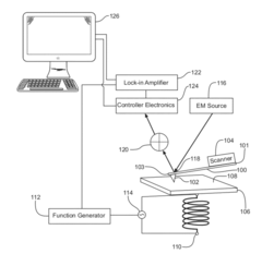
Array atomic force microscopy for enabling simultaneous multi-point and multi-modal nanoscale analyses and stimulations
PatentActiveUS20210396783A1
Innovation
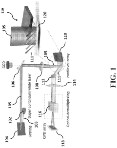
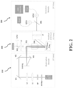
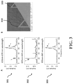
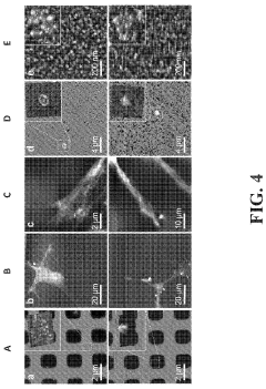
- The development of a spectral-spatially encoded array AFM (SEA-AFM) system using a supercontinuum laser and dispersive optics, which allows for simultaneous monitoring of multiple probe-sample interactions by assigning each cantilever a unique wavelength channel, minimizing crosstalk and enabling high-resolution, multiparametric imaging of morphology, hydrophobicity, and electric potential in both air and liquid.
Atomic Force Microscopy System and Method for Nanoscale Measurement
PatentActiveUS20120030846A1
Innovation
- An AFM system with a cantilever and electromagnetic coil that generates a time-varying magnetic field within the sample, allowing for imaging of various properties without bias voltage and using softer cantilevers for higher sensitivity, including electrical, dielectric, and magnetic properties, with a non-magnetic or magnetic tip.
Nanoscale Measurement Precision and Sensitivity Analysis
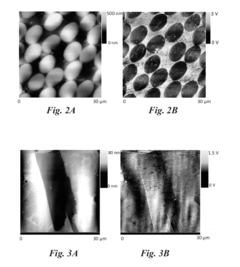
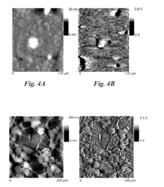
The integration of photonics with Atomic Force Microscopy (AFM) readout systems presents unprecedented opportunities for enhancing measurement precision at the nanoscale. Current AFM systems typically achieve vertical resolution in the sub-nanometer range (0.1-0.5 nm) and lateral resolution of 1-5 nm under optimal conditions. However, when incorporating photonic readout mechanisms, these parameters can be significantly improved, potentially reaching vertical resolutions below 0.05 nm and lateral resolutions approaching the atomic scale.
Sensitivity analysis of photonics-enhanced AFM systems reveals several critical factors affecting measurement precision. The signal-to-noise ratio (SNR) emerges as the primary determinant, with photonic integration offering up to 20 dB improvement over conventional electronic readout methods. This enhancement stems from the inherent immunity of optical signals to electromagnetic interference and reduced thermal noise contributions.
Quantum-limited detection schemes, particularly those employing squeezed light states, demonstrate theoretical sensitivity improvements approaching the Heisenberg limit. Recent experimental implementations have verified sensitivity enhancements of 3-7 times compared to classical detection schemes, though practical challenges in maintaining quantum coherence at room temperature remain significant barriers to widespread adoption.
Environmental factors significantly impact measurement precision in photonics-AFM hybrid systems. Temperature fluctuations of merely 0.1°C can induce drift errors of 1-2 nm, necessitating sophisticated thermal stabilization techniques. Similarly, mechanical vibrations with amplitudes as low as 0.1 nm can compromise measurement integrity, requiring advanced isolation systems that combine passive and active damping technologies.
Calibration methodologies for these hybrid systems require standardized reference materials with precisely known dimensions. Silicon gratings with pitch accuracy of ±0.1 nm serve as primary calibration standards, while atomic lattices of highly oriented pyrolytic graphite (HOPG) provide secondary verification with atomic-level precision.
Statistical analysis of measurement uncertainty in photonics-AFM systems follows the Guide to the Expression of Uncertainty in Measurement (GUM) framework. Combined standard uncertainty calculations typically incorporate contributions from thermal drift (0.2-0.5 nm), calibration uncertainty (0.1-0.3 nm), photonic detector noise (0.05-0.1 nm), and mechanical vibrations (0.1-0.3 nm). These components yield expanded uncertainty values (k=2) ranging from 0.3 to 0.8 nm for typical measurement scenarios, representing a 30-50% improvement over conventional AFM systems.
Commercialization Roadmap for Integrated Photonics-AFM Solutions
The commercialization pathway for integrated photonics-AFM solutions requires a strategic approach that balances technological innovation with market readiness. Initially, market entry should focus on research institutions and specialized industrial applications where the enhanced capabilities of photonic AFM readout systems justify premium pricing.
A phased commercialization strategy is recommended, beginning with specialized instrumentation for advanced research facilities. This allows for refinement of the technology while generating revenue and establishing brand recognition. The initial target markets should include semiconductor metrology, materials science research, and biomedical imaging applications.
Mid-term commercialization efforts should expand into broader industrial applications, particularly in quality control for nanomaterials and semiconductor manufacturing. This phase requires developing more robust, user-friendly systems with improved automation and data processing capabilities to appeal to industrial users who prioritize reliability and throughput.
Strategic partnerships will be crucial throughout the commercialization journey. Collaborations with established AFM manufacturers can provide access to existing distribution channels and customer bases. Additionally, partnerships with photonics component suppliers will ensure stable supply chains and potentially reduce production costs through economies of scale.
Intellectual property protection represents a critical foundation for successful commercialization. Companies should pursue a comprehensive patent strategy covering both the integrated system architecture and specific implementation techniques. Cross-licensing agreements may be necessary in this interdisciplinary field where existing patents may cover aspects of both photonics and AFM technologies.
Pricing strategies should evolve with market penetration. Premium pricing is appropriate for early adopters seeking cutting-edge capabilities, while more competitive pricing will become necessary as the technology matures and competition increases. Value-based pricing models that emphasize total cost of ownership advantages over conventional AFM systems will resonate with industrial customers.
Regulatory considerations vary by application sector. Medical applications will require compliance with relevant healthcare regulations, while industrial implementations may need to meet specific safety and performance standards. Early engagement with regulatory bodies can prevent costly delays in commercialization timelines.
Unlock deeper insights with Patsnap Eureka Quick Research — get a full tech report to explore trends and direct your research. Try now!
Generate Your Research Report Instantly with AI Agent
Supercharge your innovation with Patsnap Eureka AI Agent Platform!