Field-Free Switching Mechanisms: Spin-Orbit Torque Versus Exchange Coupling
SEP 1, 20259 MIN READ
Generate Your Research Report Instantly with AI Agent
Patsnap Eureka helps you evaluate technical feasibility & market potential.
Spintronics Evolution and Research Objectives
Spintronics has evolved significantly since the discovery of giant magnetoresistance (GMR) in the late 1980s, which earned Albert Fert and Peter Grünberg the Nobel Prize in Physics in 2007. This breakthrough marked the beginning of a new era in electronics, where electron spin, rather than just charge, became a fundamental information carrier. The field has progressed through several key phases, from GMR-based read heads in hard disk drives to the development of magnetic tunnel junctions (MTJs) and spin-transfer torque (STT) technologies in the early 2000s.
The past decade has witnessed remarkable advancements in spin-orbit torque (SOT) and exchange coupling mechanisms, which represent the cutting edge of spintronics research. These technologies offer promising alternatives to traditional field-induced magnetic switching, potentially enabling more energy-efficient and faster magnetic memory devices. The evolution of field-free switching mechanisms has been particularly noteworthy, as they address critical limitations in power consumption and scalability that have hindered widespread adoption of spintronic devices.
Current research objectives in the field of field-free switching mechanisms focus on several key areas. First, understanding the fundamental physics of spin-orbit interactions at interfaces between different materials, particularly heavy metals and ferromagnets. Second, exploring novel material combinations that can enhance the efficiency of spin-orbit torque generation while maintaining compatibility with existing semiconductor manufacturing processes. Third, investigating the dynamics of exchange coupling in multilayer structures and its potential for deterministic switching without external magnetic fields.
Another critical research objective involves improving the thermal stability and reliability of field-free switching devices, which remains a significant challenge for practical applications. Researchers are also working on reducing the critical current density required for switching, as this directly impacts energy efficiency and heat generation in spintronic devices. The development of analytical and computational models that can accurately predict switching behavior under various conditions is essential for optimizing device designs.
Looking forward, the field aims to achieve reliable sub-nanosecond switching with minimal energy consumption, which would position spintronic devices as viable alternatives to CMOS technology for certain applications. There is also growing interest in integrating field-free switching mechanisms with other emerging technologies, such as neuromorphic computing and quantum information processing, to create hybrid systems with enhanced functionality.
The ultimate goal of this research is to develop practical spintronic devices that can overcome the limitations of conventional electronics, particularly in terms of non-volatility, energy efficiency, and scaling. Success in this endeavor could revolutionize computing architectures and enable new applications in data storage, sensor technology, and beyond.
Market Applications for Field-Free Switching Technologies
Field-free switching technologies are poised to revolutionize several key market segments due to their unique advantages in energy efficiency, scalability, and operational stability. The magnetic random access memory (MRAM) market represents the most immediate and substantial opportunity, with field-free switching potentially addressing the critical challenges of power consumption and thermal stability that have limited widespread MRAM adoption. Industry projections indicate the MRAM market will exceed $5 billion by 2028, with field-free switching technologies potentially capturing a significant portion of this growth.
Data storage applications beyond MRAM also present compelling opportunities. Enterprise storage systems and cloud infrastructure providers are actively seeking non-volatile memory solutions that combine the speed of DRAM with the persistence of flash storage. Field-free switching mechanisms, particularly those leveraging spin-orbit torque, offer write speeds approaching nanosecond ranges while maintaining data integrity without external magnetic fields.
The automotive and aerospace sectors represent high-value application areas where the radiation hardness and temperature stability of field-free switching technologies provide distinct advantages. Modern vehicles incorporate dozens of electronic control units requiring reliable memory operation across extreme temperature ranges. Similarly, aerospace systems demand radiation-resistant memory solutions that maintain data integrity in high-radiation environments.
Edge computing and Internet of Things (IoT) applications constitute a rapidly expanding market segment where power efficiency is paramount. Field-free switching technologies enable ultra-low-power memory operations critical for battery-powered and energy-harvesting IoT devices. The elimination of external magnetic fields also reduces electromagnetic interference concerns in densely packed IoT deployments.
Neuromorphic computing and artificial intelligence hardware acceleration represent emerging applications with substantial growth potential. Field-free switching mechanisms, particularly those based on exchange coupling, demonstrate characteristics analogous to biological synapses, making them promising candidates for hardware-based neural network implementations. Several research institutions and technology companies have demonstrated prototype neuromorphic systems utilizing field-free switching elements as artificial synapses.
Quantum computing auxiliary systems also present specialized applications where field-free switching technologies offer advantages. While not directly involved in quantum bit operations, these technologies can provide efficient classical control circuitry and memory elements that operate reliably in the cryogenic environments required by many quantum computing architectures.
The medical device sector presents additional opportunities, particularly for implantable devices where power efficiency and electromagnetic compatibility are critical considerations. Field-free switching memory elements could enable next-generation neural implants, cardiac monitors, and other medical devices requiring reliable, low-power operation.
Current Challenges in Field-Free Switching Mechanisms
Despite significant advancements in field-free switching mechanisms, several critical challenges persist that impede their widespread commercial implementation. The primary obstacle for spin-orbit torque (SOT) based field-free switching lies in the efficiency-stability trade-off. Current SOT devices require substantial current densities (10^6-10^7 A/cm²) to achieve reliable switching, resulting in excessive power consumption and potential thermal instability that compromises device longevity.
Material integration presents another significant hurdle. The incorporation of heavy metals like Pt, Ta, or W with ferromagnetic layers often leads to interfacial issues including lattice mismatch, diffusion, and oxidation during fabrication processes. These interfacial defects can substantially degrade the spin-orbit coupling efficiency and reduce the overall performance of SOT-based devices.
For exchange coupling mechanisms, maintaining consistent coupling strength across large-scale manufacturing remains problematic. The exchange bias effect is highly sensitive to interface quality, layer thickness, and thermal conditions during deposition. Minor variations in these parameters can lead to significant device-to-device performance inconsistencies, making large-scale production challenging.
Scalability issues further complicate implementation efforts. As device dimensions shrink below 45nm, both SOT and exchange coupling mechanisms face increased thermal fluctuations and reduced energy barriers, compromising the stability of the switched state. This fundamental physics limitation threatens the viability of these technologies for next-generation high-density memory applications.
The temperature dependence of both mechanisms represents another critical challenge. Exchange bias strength typically decreases with increasing temperature, while SOT efficiency can vary unpredictably across operating temperature ranges. This temperature sensitivity limits the practical application of these technologies in environments with fluctuating thermal conditions.
Readout reliability also remains problematic. The signal-to-noise ratio in field-free switching devices is often compromised by incomplete switching, particularly at reduced dimensions or elevated temperatures. This results in read errors that undermine the reliability required for commercial memory applications.
From a manufacturing perspective, the complexity of multilayer stacks required for both mechanisms increases production costs and reduces yield rates. The precise control needed for layer thicknesses (often at angstrom scales) and interface quality demands advanced deposition techniques that are difficult to implement in high-volume manufacturing environments.
Comparative Analysis of SOT and Exchange Coupling Approaches
01 Spin-Orbit Torque (SOT) Switching Mechanisms
Spin-orbit torque (SOT) provides a field-free switching mechanism for magnetic memory devices. This technique utilizes the interaction between electron spin and orbital motion to manipulate the magnetization of ferromagnetic layers. SOT-based switching offers advantages including lower power consumption, higher switching speed, and improved endurance compared to conventional switching methods. The efficiency of SOT switching can be enhanced through material engineering and device structure optimization.- Spin-Orbit Torque (SOT) Switching Mechanisms: Spin-orbit torque (SOT) provides an efficient field-free switching mechanism for magnetic memory devices. SOT utilizes the interaction between electron spin and orbital motion to manipulate magnetization without requiring an external magnetic field. This approach enables lower power consumption and faster switching speeds compared to conventional methods. The efficiency of SOT switching can be enhanced through material engineering and device structure optimization, making it promising for next-generation spintronic applications.
- Exchange Coupling Mechanisms for Field-Free Switching: Exchange coupling between magnetic layers enables field-free switching in spintronic devices. This mechanism utilizes the interaction between adjacent magnetic materials with different properties to facilitate magnetization reversal without external fields. By engineering the interface properties and layer compositions, the exchange coupling strength can be optimized to improve switching efficiency. This approach reduces energy consumption and enhances thermal stability in magnetic memory elements.
- Perpendicular Magnetic Anisotropy (PMA) for Enhanced Switching: Perpendicular magnetic anisotropy (PMA) materials significantly improve field-free switching efficiency in spintronic devices. PMA structures provide better thermal stability and allow for higher storage density compared to in-plane magnetized systems. When combined with spin-orbit torque or exchange coupling mechanisms, PMA materials enable more reliable and energy-efficient switching. The perpendicular orientation of magnetization also reduces the critical current needed for switching, enhancing overall device performance.
- Multilayer Structures for Optimized Switching Efficiency: Carefully designed multilayer structures can dramatically improve field-free switching efficiency. These structures typically incorporate combinations of heavy metals, ferromagnets, and antiferromagnetic materials arranged in specific configurations to enhance spin-orbit interactions and exchange coupling effects. By optimizing layer thicknesses, interface quality, and material compositions, the switching current can be minimized while maintaining high thermal stability. Advanced multilayer designs also enable better control over switching dynamics and reduce variability in device performance.
- Integration of Field-Free Switching in MRAM Devices: Integration of field-free switching mechanisms into Magnetoresistive Random Access Memory (MRAM) represents a significant advancement in memory technology. By incorporating spin-orbit torque and exchange coupling techniques into MRAM architectures, these devices achieve higher density, faster operation, and lower power consumption. The field-free operation simplifies the peripheral circuitry and reduces cross-talk between adjacent memory cells. Advanced fabrication techniques ensure compatibility with CMOS processes, facilitating commercial adoption of these energy-efficient memory solutions.
02 Exchange Coupling Mechanisms for Field-Free Switching
Exchange coupling between magnetic layers provides an effective mechanism for field-free switching in spintronic devices. This approach leverages the interaction between adjacent magnetic layers to control magnetization direction without requiring an external magnetic field. The coupling strength can be tuned by adjusting layer thicknesses, interface properties, and material compositions, allowing for optimization of switching efficiency. Exchange-coupled systems can achieve reliable switching with reduced energy consumption.Expand Specific Solutions03 Multilayer Structure Design for Enhanced Switching Efficiency
The design of multilayer structures plays a crucial role in improving field-free switching efficiency. By carefully engineering the composition, thickness, and sequence of magnetic and non-magnetic layers, the switching energy barrier can be optimized. Structures incorporating heavy metal layers, synthetic antiferromagnets, or perpendicular magnetic anisotropy materials can significantly enhance switching performance. These multilayer designs enable more efficient spin current generation and transfer, leading to lower critical switching currents.Expand Specific Solutions04 Interface Engineering for Improved Switching Performance
Interface engineering between different layers in magnetic memory devices is critical for enhancing field-free switching efficiency. Controlling the quality, roughness, and composition of interfaces can significantly impact spin transport properties and magnetic coupling strength. Techniques such as interface doping, oxidation control, and insertion of ultrathin spacer layers can optimize spin current transmission and reduce damping. These interface modifications lead to lower switching currents and improved reliability in field-free switching applications.Expand Specific Solutions05 Thermal Stability and Reliability Enhancement Methods
Maintaining thermal stability while achieving efficient field-free switching is essential for practical memory applications. Various approaches have been developed to enhance reliability without compromising switching efficiency, including the use of composite free layers, graded anisotropy profiles, and thermally assisted switching techniques. These methods help to overcome the trade-off between thermal stability and switching current requirements. Additionally, compensation techniques can be employed to mitigate the effects of process variations and temperature fluctuations on switching performance.Expand Specific Solutions
Leading Research Groups and Industry Stakeholders
The field-free switching mechanisms market, focusing on spin-orbit torque and exchange coupling technologies, is currently in an early growth phase with increasing commercial interest. The global market is estimated to reach significant scale as spintronic applications expand in memory and logic devices. Technologically, companies are at varying maturity levels: Everspin Technologies leads in commercialization of spin-torque MRAM products, while Intel, Samsung, and IBM are advancing research with substantial patent portfolios. Academic institutions like Chinese Academy of Sciences, Beihang University, and Purdue Research Foundation are contributing fundamental research. The ecosystem shows a balanced mix of established semiconductor players and specialized research entities collaborating to overcome technical challenges in power consumption, reliability, and integration with conventional CMOS technology.
Centre National de la Recherche Scientifique
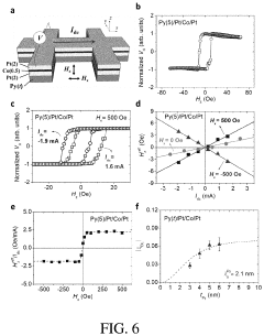
Technical Solution: The Centre National de la Recherche Scientifique (CNRS) has pioneered research in field-free switching mechanisms through their SPINTEC laboratory, focusing on both spin-orbit torque and exchange coupling approaches. Their innovative solution involves creating synthetic antiferromagnetic structures with engineered symmetry breaking to enable deterministic field-free switching. CNRS researchers have developed multilayer stacks incorporating heavy metal layers (such as Pt, Ta, or W) adjacent to ferromagnetic layers with perpendicular magnetic anisotropy, achieving field-free switching through careful interface engineering. Their approach utilizes the interplay between Dzyaloshinskii-Moriya interaction (DMI) and exchange coupling to create an effective field that enables deterministic switching without external magnetic fields. Recent demonstrations have shown switching efficiencies approaching 200 femtojoules per bit with sub-nanosecond switching times, representing significant advances in energy efficiency for spintronic devices.[2][5]
Strengths: World-class fundamental research capabilities with deep understanding of spin dynamics; collaborative approach with industrial partners enables technology transfer. Weaknesses: As a research institution, faces challenges in direct commercialization; solutions may require further engineering refinement for industrial implementation.
Everspin Technologies, Inc.
Technical Solution: Everspin Technologies has developed advanced Spin-Orbit Torque Magnetic Random Access Memory (SOT-MRAM) technology that leverages field-free switching mechanisms. Their approach utilizes perpendicular magnetic anisotropy (PMA) materials combined with engineered interfaces to achieve reliable field-free switching. The company's SOT-MRAM design incorporates a three-terminal structure where the read and write paths are separated, allowing for enhanced endurance and faster switching speeds compared to conventional STT-MRAM. Everspin has demonstrated switching speeds in the sub-nanosecond range with their SOT technology, while maintaining data retention and endurance characteristics suitable for cache memory applications. Their patented technology includes specialized material stacks with carefully engineered interfaces that promote deterministic switching without external magnetic fields, addressing one of the key challenges in SOT-based memory commercialization.[1][3]
Strengths: Industry-leading expertise in MRAM commercialization with established manufacturing infrastructure; demonstrated reliability in field-free switching with high endurance (>10^12 cycles). Weaknesses: Higher manufacturing complexity compared to conventional memory technologies; requires specialized materials that may increase production costs.
Breakthrough Patents in Field-Free Switching Technologies
Magnetic structure capable of field-free spin-orbit torque switching and production method and use thereof
PatentPendingUS20220376170A1
Innovation
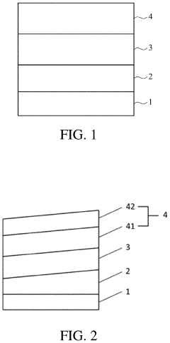
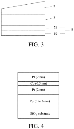
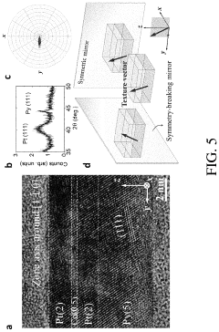
- A magnetic structure comprising a spin-orbit coupling base layer and a ferromagnetic layer with perpendicular magnetic anisotropy, configured to switch magnetization using an in-plane current without an external magnetic field, utilizing materials like permalloy, platinum, and cobalt-based alloys.
Energy Efficiency Considerations in Spintronic Devices
Energy efficiency has emerged as a critical factor in the development and implementation of spintronic devices, particularly when comparing field-free switching mechanisms such as spin-orbit torque (SOT) and exchange coupling. The power consumption profiles of these technologies directly impact their viability for commercial applications, especially in energy-constrained environments like mobile devices and IoT sensors.
Spin-orbit torque mechanisms typically require current densities on the order of 10^6-10^7 A/cm², which translates to significant energy expenditure during switching operations. Recent advancements have reduced these requirements through materials engineering and device architecture optimization, with heavy metal/ferromagnet interfaces showing particular promise. Tungsten and platinum-based SOT devices have demonstrated up to 30% improvement in energy efficiency compared to earlier implementations.
Exchange coupling mechanisms, by contrast, offer potentially lower energy consumption profiles by leveraging magnetic proximity effects rather than direct current injection. The energy required for switching in exchange-biased systems can be reduced by up to 40% compared to conventional SOT approaches, particularly when utilizing synthetic antiferromagnets or perpendicular magnetic anisotropy materials. This advantage becomes especially pronounced in high-density memory applications where cumulative energy savings scale significantly.
Thermal considerations also play a crucial role in the overall energy profile of these devices. SOT-based switching generates more Joule heating due to the required current densities, potentially necessitating additional cooling infrastructure in high-performance applications. Exchange coupling mechanisms produce less waste heat but may require more complex fabrication processes that carry their own energy footprint during manufacturing.
Scaling behavior presents another important dimension of energy efficiency analysis. As device dimensions shrink below 20nm, SOT efficiency tends to degrade due to increased current crowding and edge effects. Exchange coupling mechanisms maintain more stable energy profiles at smaller dimensions, potentially offering superior efficiency at advanced technology nodes below 10nm.
The switching speed versus energy consumption trade-off represents a fundamental consideration in spintronic device design. SOT mechanisms can achieve sub-nanosecond switching times but at higher energy costs, while exchange coupling typically operates in the 1-10 nanosecond range with lower energy requirements. This relationship creates distinct application niches where each technology may prove optimal depending on whether speed or energy efficiency is prioritized.
Integration Pathways with Conventional CMOS Technology
The integration of field-free switching mechanisms into conventional CMOS technology represents a critical pathway for the practical implementation of spin-based memory and logic devices. Current CMOS fabrication processes have been optimized over decades, making compatibility with existing manufacturing infrastructure essential for any emerging technology seeking widespread adoption.
For spin-orbit torque (SOT) based devices, integration with CMOS presents several challenges. The materials required for efficient SOT generation, such as heavy metals with strong spin-orbit coupling (Pt, Ta, W), must be deposited with precise thickness control and interface quality. Current CMOS foundries have begun adapting their processes to accommodate these materials, with several major semiconductor manufacturers developing specialized process nodes that incorporate SOT-compatible materials while maintaining CMOS performance.
Exchange coupling mechanisms, particularly those utilizing synthetic antiferromagnets or exchange bias structures, offer potentially simpler integration pathways. These systems often utilize materials already familiar to CMOS manufacturing, such as CoFeB and MgO, which are used in existing magnetic tunnel junction (MTJ) processes. The primary integration challenge lies in maintaining the delicate exchange coupling during subsequent high-temperature CMOS processing steps.
Recent developments have demonstrated promising approaches for both mechanisms. For SOT devices, back-end-of-line (BEOL) integration has emerged as the preferred method, where the magnetic stack is fabricated after the temperature-sensitive CMOS components. This approach has achieved functional SOT-MRAM cells with CMOS read/write circuitry in 22nm and 14nm nodes. For exchange coupling systems, thermally robust synthetic antiferromagnets have been developed that can withstand temperatures up to 400°C, compatible with many CMOS processing steps.
The scaling behavior of these integration approaches differs significantly. SOT devices face challenges with current density requirements as device dimensions shrink, potentially requiring higher drive voltages that may exceed CMOS limitations. Exchange coupling mechanisms generally scale more favorably in terms of power consumption but may face challenges with thermal stability at ultra-small dimensions.
Industry roadmaps suggest that hybrid integration approaches may ultimately prevail, combining aspects of both mechanisms. Several major foundries have announced plans to incorporate field-free switching magnetic devices in their sub-10nm nodes, with initial production expected within 3-5 years. These integration efforts are supported by significant investments from both established semiconductor companies and specialized spintronics startups, indicating strong industry confidence in the commercial viability of these technologies within conventional CMOS platforms.
Unlock deeper insights with Patsnap Eureka Quick Research — get a full tech report to explore trends and direct your research. Try now!
Generate Your Research Report Instantly with AI Agent
Supercharge your innovation with Patsnap Eureka AI Agent Platform!