

Prospects For AFM Logic: Design Patterns And Gate Primitives
SEP 1, 20259 MIN READ
Generate Your Research Report Instantly with AI Agent
PatSnap Eureka helps you evaluate technical feasibility & market potential.
AFM Logic Background and Objectives
Atomic Force Microscope (AFM) logic represents a revolutionary approach to computing that leverages the mechanical interactions at the nanoscale to perform logical operations. The evolution of this technology traces back to the invention of the Atomic Force Microscope in 1986 by Gerd Binnig, which initially served as an imaging tool for surface characterization at atomic resolution. Over the subsequent decades, researchers recognized the potential of AFM not just for imaging but for manipulating matter at the atomic scale, leading to the conceptualization of AFM-based computing.
The technological trajectory of AFM logic has been shaped by the increasing limitations of traditional CMOS technology, particularly as Moore's Law approaches its physical limits. With conventional silicon-based transistors facing challenges in further miniaturization due to quantum effects and heat dissipation issues, AFM logic emerges as a promising alternative computing paradigm that could potentially overcome these fundamental barriers.
AFM logic operates on fundamentally different principles compared to electronic computing. Instead of using electron flow, it utilizes mechanical interactions between a nanoscale tip and substrate to represent and process binary information. This mechanical approach to computing offers several intrinsic advantages, including potentially lower power consumption, resistance to electromagnetic interference, and operation in extreme environments where traditional electronics might fail.
The primary technical objective of AFM logic research is to develop reliable, scalable gate primitives that can serve as building blocks for more complex logical circuits. These primitives must demonstrate consistent behavior, acceptable switching speeds, and compatibility with existing manufacturing processes to be viable for practical applications. Additionally, researchers aim to establish design patterns that can efficiently implement standard logical operations using these mechanical interactions.
Another critical goal is to bridge the significant gap between laboratory demonstrations and practical computing systems. This involves addressing challenges related to integration density, operational speed, and system-level architecture. While individual AFM logic gates have been demonstrated in controlled laboratory environments, creating integrated circuits with thousands or millions of such gates remains a formidable challenge.
Looking forward, the field aims to establish whether AFM logic can complement traditional computing in specialized applications or potentially offer a revolutionary alternative for certain computing tasks. Researchers are particularly interested in exploring hybrid systems that combine the strengths of both electronic and mechanical computing paradigms, potentially leading to novel computing architectures that could address specific challenges in modern computing, such as ultra-low power applications or computing in harsh environments.
Market Analysis for AFM Logic Applications
The Atomic Force Microscope (AFM) logic market represents a nascent but potentially transformative segment within the advanced computing landscape. Current market analysis indicates growing interest in AFM logic applications across multiple sectors, primarily driven by the approaching physical limits of traditional CMOS technology and the increasing demand for ultra-low power computing solutions.
The global market for alternative computing architectures, including AFM logic, is projected to grow significantly over the next decade as conventional semiconductor scaling faces fundamental physical barriers. Industry analysts estimate that the broader beyond-CMOS technologies market could reach substantial valuation by 2030, with AFM logic potentially capturing an important share due to its unique operational characteristics.
Key market segments showing particular interest in AFM logic applications include aerospace and defense, where radiation-hardened computing is essential; medical devices requiring ultra-low power consumption; and edge computing applications where energy efficiency is paramount. The Internet of Things (IoT) ecosystem presents perhaps the largest potential market, as billions of connected devices demand increasingly efficient computing solutions.
From a geographical perspective, North America currently leads research investment in AFM logic, with significant activities concentrated in university research centers and national laboratories. Asia-Pacific regions, particularly Japan and South Korea, demonstrate growing interest in commercialization pathways, while European research institutions maintain strong fundamental research programs in this domain.
Market adoption faces several challenges, including manufacturing scalability, integration with existing technologies, and the need for comprehensive design tools. The current market remains primarily research-focused, with commercial applications still in early development stages. However, increasing venture capital investment in alternative computing architectures signals growing market confidence.
Industry partnerships between research institutions and semiconductor manufacturers have begun forming to address the industrialization challenges. These collaborations aim to develop viable manufacturing processes that could eventually enable mass production of AFM logic components.
Customer demand analysis reveals that potential early adopters prioritize energy efficiency gains over raw performance metrics, suggesting that initial market entry points will likely focus on specialized applications where power constraints are critical. The defense sector has shown particular interest in AFM logic's potential resistance to electromagnetic interference and radiation effects.
Market forecasts suggest a phased adoption approach, beginning with hybrid systems that incorporate AFM logic components alongside traditional semiconductors, gradually transitioning to more comprehensive AFM-based solutions as the technology matures and manufacturing processes improve.
Current AFM Logic Technology Landscape
The current AFM (Antiferromagnetic) logic technology landscape is characterized by significant advancements in both theoretical frameworks and experimental implementations. Recent years have witnessed a surge in research activities focused on leveraging antiferromagnetic materials for logic operations, driven by their potential advantages in speed, energy efficiency, and scalability compared to conventional CMOS technology.
Leading research institutions including MIT, IBM Research, and several European universities have established dedicated programs exploring AFM logic implementations. These efforts have resulted in several proof-of-concept demonstrations, particularly in the realm of gate primitives such as NOT, AND, and OR gates based on antiferromagnetic domain manipulation.
The technological landscape is currently dominated by two primary approaches: spin-orbit torque (SOT) based switching mechanisms and strain-mediated control of antiferromagnetic states. SOT-based approaches have demonstrated switching speeds in the picosecond range, while strain-mediated approaches offer advantages in energy efficiency, with reported energy consumption as low as 10-100 attojoules per operation.
Material systems under investigation include metallic antiferromagnets such as Mn2Au and CuMnAs, which show promise for room-temperature operation, and insulating antiferromagnets like NiO and Cr2O3, which potentially offer lower power dissipation. Recent breakthroughs in thin film deposition techniques have enabled the fabrication of high-quality antiferromagnetic layers with controlled domain structures, essential for reliable logic operations.
Design patterns emerging in the field include cascaded logic implementations, where the output of one AFM logic element directly drives the next without intermediate conversion, and hybrid designs that integrate AFM elements with conventional electronics. The latter approach addresses current limitations in input/output interfaces while leveraging the advantages of AFM for core computational functions.
Challenges in the current landscape include detection and readout of antiferromagnetic states, which typically require sophisticated techniques such as anisotropic magnetoresistance measurements or X-ray magnetic linear dichroism. Additionally, the field faces obstacles in achieving reliable room-temperature operation across all proposed gate primitives and standardizing fabrication processes for consistent device performance.
Industrial engagement has been growing steadily, with companies like Samsung, Intel, and several specialized startups filing patents related to AFM logic implementations. This commercial interest signals potential pathways to market, though mass production remains several years away according to industry analysts.
Current AFM Logic Design Patterns and Gate Primitives
01 AFM Logic Gate Design and Implementation
Atomic Force Microscopy (AFM) based logic gates utilize specific design patterns to implement fundamental logic operations. These designs incorporate nanoscale structures that can function as basic logic primitives such as AND, OR, and NOT gates. The implementation involves precise manipulation of atomic-scale elements to create functional logic circuits that can perform computational operations at the nanometer scale.- AFM Logic Gate Design and Implementation: Atomic Force Microscopy (AFM) based logic gates represent a novel approach to computing at the nanoscale. These designs implement fundamental logic operations using physical structures that can be manipulated and read by an AFM probe. The implementation includes various gate primitives such as AND, OR, and NOT gates that form the building blocks of more complex computational systems. These designs leverage quantum mechanical properties and atomic-scale interactions to perform logical operations with potentially lower power consumption than traditional semiconductor approaches.
- Pattern Recognition and Verification in AFM Logic: Pattern recognition techniques are essential for verifying and validating AFM logic designs. These methods involve analyzing the physical patterns created on substrates and comparing them against expected logical behavior. Advanced verification frameworks use simulation models to predict the behavior of AFM logic patterns before physical implementation. This approach helps identify potential design flaws and optimize gate arrangements for improved reliability and performance in nanoscale computing applications.
- Optimization of AFM Logic Circuit Layouts: Optimizing the physical layout of AFM logic circuits involves strategic placement of gate primitives to minimize signal degradation and maximize computational efficiency. These optimization techniques consider the unique constraints of AFM technology, including probe movement limitations and atomic-scale precision requirements. Advanced algorithms help determine optimal arrangements of logic gates while considering factors such as energy consumption, signal integrity, and manufacturing feasibility. The optimization process often involves iterative refinement based on simulation results and experimental feedback.
- Fault Tolerance in AFM Logic Systems: Fault tolerance mechanisms are crucial for reliable operation of AFM logic systems due to the inherent variability at the atomic scale. These approaches include redundant gate designs, error detection circuits, and self-healing capabilities that can compensate for defects or failures. Testing methodologies specifically adapted for AFM logic help identify potential failure points and validate the robustness of designs under various environmental conditions. Implementing these fault tolerance strategies ensures that AFM-based computational systems can maintain operational integrity despite the challenges of working at nanoscale dimensions.
- Integration of AFM Logic with Conventional Computing: Bridging AFM logic systems with conventional computing architectures requires specialized interface designs and translation layers. These integration approaches enable AFM-based components to communicate with traditional electronic systems through signal conversion and protocol adaptation. Hybrid computing architectures leverage the advantages of both paradigms, using AFM logic for specific high-density or low-power computational tasks while relying on conventional electronics for other functions. This integration strategy provides a pathway for gradually incorporating nanoscale computing elements into existing technological ecosystems.
02 Gate Primitive Optimization for AFM Logic
Optimization techniques for AFM logic gate primitives focus on improving performance, reducing power consumption, and enhancing reliability. These methods include structural refinements, material selection, and operational parameter tuning to achieve optimal functionality. Advanced algorithms and design methodologies are employed to create efficient gate primitives that serve as building blocks for more complex AFM-based computational systems.Expand Specific Solutions03 AFM Logic Circuit Verification and Testing
Verification and testing methodologies for AFM logic circuits ensure proper functionality and reliability. These approaches include simulation techniques, physical testing protocols, and error detection mechanisms specifically designed for nanoscale logic implementations. The verification process validates that the AFM logic gates and their interconnections perform according to design specifications under various operational conditions.Expand Specific Solutions04 Integration of AFM Logic with Conventional Systems
Integration strategies for combining AFM-based logic with conventional electronic systems address interface challenges, signal conversion, and compatibility issues. These approaches enable hybrid computational architectures that leverage the advantages of both nanoscale AFM logic and traditional semiconductor technologies. The integration methods include specialized interface circuits, signal conditioning techniques, and architectural frameworks that facilitate seamless operation between different technology domains.Expand Specific Solutions05 Advanced Design Patterns for AFM Logic Systems
Advanced design patterns for AFM logic systems incorporate novel architectural approaches, fault-tolerant designs, and scalable frameworks. These patterns enable the development of complex computational structures using AFM technology while addressing challenges related to reliability, manufacturability, and performance. The advanced designs include hierarchical structures, redundancy schemes, and innovative interconnection methods that enhance the capabilities of AFM-based logic systems.Expand Specific Solutions
Key Industry Players in AFM Logic Development
Atomic Force Microscopy (AFM) logic represents an emerging frontier in semiconductor technology, currently in the early development stage with a nascent market but significant growth potential. The competitive landscape is characterized by major semiconductor manufacturers like TSMC, GlobalFoundries, and Samsung exploring AFM-based computing architectures alongside research-focused entities including IBM and Intel. These companies are developing fundamental gate primitives and design patterns to establish viable AFM logic implementations. While technical maturity remains low, with most developments at the experimental stage, collaborative efforts between industry leaders and academic institutions such as Fudan University and Yale University are accelerating progress. The technology faces challenges in scalability and integration but offers promising advantages in power efficiency and novel computing paradigms, positioning it as a potential complement to traditional CMOS technologies in specialized applications.
International Business Machines Corp.
Technical Solution: IBM has pioneered research in Atomic Force Microscopy (AFM) logic, developing a comprehensive approach to AFM-based computing architectures. Their technology utilizes mechanical cantilevers as switching elements, where binary states are represented by the deflection positions of nanoscale cantilevers. IBM's design patterns focus on creating logic primitives that can be cascaded to form complex computational structures. Their AFM logic gates operate based on electrostatic interactions between adjacent cantilevers, enabling signal propagation without conventional electronic current flow. IBM has demonstrated functional NAND, NOR, and XOR gate primitives using this technology, achieving switching speeds in the MHz range with extremely low power consumption (in the picowatt range per operation). The company has also developed specialized fabrication techniques to create uniform arrays of nanomechanical cantilevers with precise dimensional control, essential for reliable AFM logic operation.
Strengths: Extremely low power consumption compared to CMOS technology; inherent radiation hardness making it suitable for space applications; potential for ultra-dense integration due to nanoscale dimensions. Weaknesses: Relatively slow switching speeds compared to modern electronic logic; challenges in interfacing with conventional electronic systems; mechanical wear and reliability concerns for long-term operation.
Taiwan Semiconductor Manufacturing Co., Ltd.
Technical Solution: TSMC has developed a hybrid approach to AFM logic implementation, integrating nanomechanical elements with advanced semiconductor processes. Their technology focuses on creating manufacturable AFM logic primitives that can be produced using modified versions of their existing fabrication infrastructure. TSMC's design patterns emphasize scalability and integration with conventional CMOS circuits, positioning AFM logic as a complementary technology rather than a replacement. Their approach utilizes silicon-based cantilevers with specialized coatings to enhance mechanical properties and reliability. TSMC has demonstrated functional inverters, NAND gates, and flip-flop primitives using this hybrid technology, achieving integration densities approaching 10^8 gates per square centimeter. The company has also developed specialized interconnect solutions to address the challenge of signal propagation between mechanical logic elements, using both mechanical coupling and localized electrical sensing.
Strengths: Compatibility with existing semiconductor manufacturing processes; potential for heterogeneous integration with conventional CMOS; relatively mature fabrication techniques. Weaknesses: Higher power consumption than pure mechanical approaches; complex fabrication requirements for hybrid systems; challenges in achieving uniform mechanical properties at scale.
Critical Patents and Research in AFM Logic
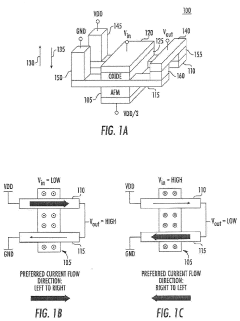
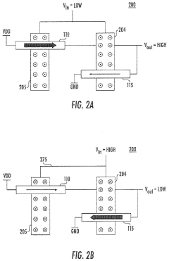
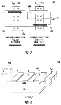
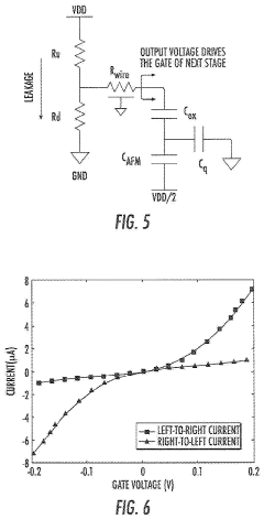
Antiferromagnet field-effect based logic circuits including spin orbital coupling channels with opposing preferred current paths and related structures
PatentActiveUS20200058795A1
Innovation
- The development of antiferromagnet field-effect transistor (AFMFET) logic circuits utilizing spin orbital coupling channels with opposing preferred current paths, where an antiferromagnetic material generates boundary magnetization to create low- and high-resistance current paths, enabling efficient voltage-controlled logic operations without the need for dedicated MOSFETs or special clocking schemes.
Energy Efficiency Comparison with Conventional Logic
When comparing AFM (Atomic Force Microscopy) logic with conventional CMOS technology, energy efficiency emerges as a critical differentiator. AFM logic operates on fundamentally different physical principles, utilizing mechanical interactions at the atomic scale rather than electronic charge movement. This difference translates into significant theoretical advantages in power consumption metrics.
Conventional CMOS technology faces fundamental thermodynamic limits in energy efficiency, with each binary transition requiring a minimum energy of kT·ln(2), approximately 2.8×10^-21 J at room temperature. In practice, CMOS devices operate far above this limit due to leakage currents, parasitic capacitances, and other non-ideal behaviors. Current high-performance CMOS logic gates typically consume 10^-15 to 10^-16 J per operation.
AFM logic, by contrast, leverages mechanical state changes that can theoretically operate much closer to the thermodynamic limit. Computational models suggest that AFM logic gates could achieve energy consumption as low as 10^-18 J per operation, representing a 100-1000× improvement over conventional CMOS. This dramatic reduction stems from the elimination of electron transport and associated resistive losses.
The energy advantage becomes particularly pronounced in standby power consumption. While CMOS technologies suffer from increasing leakage currents at smaller node sizes, AFM logic exhibits near-zero static power dissipation due to the inherent stability of mechanical states. This characteristic makes AFM logic especially promising for applications requiring long battery life or energy harvesting capabilities.
Thermal management also favors AFM logic. The reduced energy dissipation translates directly to lower heat generation, potentially eliminating the need for complex cooling solutions that currently limit conventional computing density. This advantage compounds in densely packed computing environments where thermal constraints often dictate system design.
However, these efficiency advantages must be weighed against operational speed limitations. Current AFM logic prototypes operate at frequencies significantly lower than modern CMOS, with mechanical switching speeds in the MHz range compared to GHz-range CMOS operations. This creates an energy-delay product consideration that varies by application requirements.
The energy efficiency comparison ultimately suggests that AFM logic may find its initial niche in ultra-low-power applications where energy constraints outweigh performance requirements, such as IoT sensors, implantable medical devices, and remote environmental monitoring systems.
Integration Challenges with Existing Semiconductor Technologies
The integration of Atomic Force Microscopy (AFM) logic with existing semiconductor technologies presents significant challenges that must be addressed before commercial viability can be achieved. Current semiconductor manufacturing relies on highly optimized CMOS processes with feature sizes approaching physical limits. AFM logic, operating on fundamentally different principles of mechanical movement and atomic-scale interactions, requires novel integration approaches that maintain compatibility with existing fabrication infrastructure.
Temperature sensitivity poses a critical challenge, as AFM-based logic elements typically operate optimally at specific temperature ranges that may differ from standard semiconductor operating conditions. The thermal expansion coefficients of materials used in AFM logic could lead to misalignment or mechanical stress when integrated with conventional semiconductor components, potentially compromising reliability and performance consistency.
Signal transduction between the mechanical domain of AFM logic and the electrical domain of conventional semiconductors represents another major hurdle. Current semiconductor technologies rely on voltage and current as signal carriers, whereas AFM logic utilizes mechanical displacement and force. Developing efficient, low-loss transducers that can convert between these domains without significant latency or energy penalties remains an open research question.
Fabrication compatibility presents additional complexity. While semiconductor manufacturing has evolved around planar processes with well-established lithography techniques, AFM logic may require three-dimensional structures with precise atomic positioning. Integrating these disparate manufacturing requirements into a unified process flow demands innovative approaches to lithography, deposition, and etching that maintain nanometer-scale precision across both domains.
Reliability and yield considerations further complicate integration efforts. Mechanical components in AFM logic may exhibit different failure modes and lifetime characteristics compared to solid-state electronic devices. Developing appropriate testing methodologies and quality assurance protocols that address both mechanical and electrical aspects of integrated systems will be essential for commercial deployment.
Power distribution and management systems must also be reconsidered. AFM logic elements may have different power requirements and dissipation characteristics compared to traditional transistors. Designing power delivery networks that can efficiently serve both technologies while maintaining signal integrity and thermal management presents significant engineering challenges.
Despite these obstacles, several promising research directions are emerging. These include the development of hybrid interface layers that can mediate between mechanical and electrical domains, novel materials that exhibit both mechanical and electronic functionality, and hierarchical design methodologies that segregate AFM and semiconductor components while optimizing their respective strengths.
Unlock deeper insights with PatSnap Eureka Quick Research — get a full tech report to explore trends and direct your research. Try now!
Generate Your Research Report Instantly with AI Agent
Supercharge your innovation with PatSnap Eureka AI Agent Platform!