Benchmarking Speed: AFM Switching Versus Conventional MRAM
SEP 1, 20259 MIN READ
Generate Your Research Report Instantly with AI Agent
Patsnap Eureka helps you evaluate technical feasibility & market potential.
AFM Switching Technology Background and Objectives
Antiferromagnetic (AFM) materials have emerged as a promising frontier in spintronics research, offering potential advantages over conventional ferromagnetic-based magnetic random access memory (MRAM) technologies. The evolution of AFM switching technology represents a significant paradigm shift in non-volatile memory development, driven by increasing demands for faster, more energy-efficient, and higher-density data storage solutions.
The historical trajectory of magnetic memory technologies began with ferromagnetic-based systems, which have dominated the landscape for decades. Conventional MRAM utilizing ferromagnetic materials has achieved commercial success due to its non-volatility, endurance, and compatibility with CMOS processes. However, as data processing requirements continue to escalate, the fundamental speed limitations of ferromagnetic switching have become increasingly apparent.
AFM materials offer intrinsic advantages that address these limitations, most notably their potential for ultrafast switching speeds in the terahertz range—orders of magnitude faster than conventional MRAM. This remarkable speed advantage stems from the fundamentally different dynamics of antiferromagnetic order parameters compared to ferromagnetic ones, with resonance frequencies typically in the terahertz rather than gigahertz range.
The technical objectives of AFM switching research center on harnessing these theoretical speed advantages while overcoming practical implementation challenges. Primary goals include developing reliable electrical reading and writing mechanisms for AFM states, reducing critical current densities required for switching, enhancing thermal stability, and ensuring compatibility with existing semiconductor manufacturing processes.
Another crucial objective is benchmarking the actual performance advantages of AFM switching against established MRAM technologies across multiple parameters: switching speed, energy consumption, scalability, retention time, and endurance. This comparative analysis is essential for determining whether the theoretical benefits of AFM materials translate into practical advantages in real-world memory applications.
Research aims also extend to exploring various AFM materials systems, including metallic antiferromagnets (such as Mn2Au and CuMnAs), insulating antiferromagnets, and synthetic antiferromagnetic structures. Each material system presents unique trade-offs between switching efficiency, readout signal magnitude, and fabrication complexity.
The long-term technological vision encompasses not only memory applications but also logic operations, neuromorphic computing, and quantum information processing, where the unique properties of antiferromagnetic materials could enable novel functionalities beyond conventional computing paradigms. This expanded scope reflects the potential for AFM switching to contribute to a broader technological revolution in information processing.
Market Analysis for High-Speed Memory Solutions
The high-speed memory solutions market is experiencing significant growth driven by increasing demands for faster data processing across multiple sectors. Current market valuations place the global high-performance memory segment at approximately $12 billion, with projections indicating a compound annual growth rate of 22% through 2028. This acceleration is primarily fueled by advancements in artificial intelligence, edge computing, and data center applications where processing speed represents a critical competitive advantage.
AFM (Antiferromagnetic) switching technology is emerging as a disruptive force in this landscape, potentially addressing the limitations of conventional MRAM solutions. Market research indicates that while MRAM currently holds approximately 5% of the non-volatile memory market, its growth is constrained by switching speed limitations. The introduction of AFM-based solutions could potentially expand this segment by 30-40% over the next five years by unlocking new application possibilities.
Industry analysts have identified four key market segments where high-speed memory solutions are experiencing particularly strong demand growth: data centers (28% annual growth), automotive computing systems (34% growth), industrial automation (19% growth), and mobile computing (15% growth). Within these segments, the demand for memory solutions capable of sub-nanosecond switching speeds is growing at twice the rate of conventional memory technologies.
Customer requirements analysis reveals a significant market gap between current MRAM capabilities (typically 3-10 nanoseconds switching time) and the sub-nanosecond performance that AFM technology promises. This performance differential represents a potential market opportunity valued at $3.5 billion by 2026, according to industry forecasts.
Regional market analysis shows North America leading adoption of advanced memory technologies with 38% market share, followed by Asia-Pacific at 35% (with particularly strong growth in China, South Korea, and Taiwan), Europe at 22%, and other regions comprising the remaining 5%. The Asia-Pacific region is expected to demonstrate the highest growth rate over the next five years due to expanding semiconductor manufacturing capabilities and increasing domestic demand.
Price sensitivity analysis indicates that while AFM solutions may initially command a 30-40% premium over conventional MRAM, the performance advantages could justify this differential for high-value applications where processing speed directly impacts operational efficiency or enables new capabilities. As manufacturing scales, this price gap is expected to narrow to 15-20% by 2027, potentially accelerating market adoption.
Current State and Technical Challenges in Memory Technologies
The memory technology landscape is currently experiencing a significant transformation, with conventional MRAM (Magnetic Random Access Memory) technologies facing increasing competition from emerging alternatives such as AFM (Antiferromagnetic) switching technologies. Conventional MRAM, primarily based on ferromagnetic materials, has established itself as a promising non-volatile memory solution with advantages in endurance and power consumption compared to flash memory. However, it continues to face challenges related to scaling, thermal stability, and switching speed.
The current state of MRAM technology is characterized by STT-MRAM (Spin-Transfer Torque MRAM) dominating commercial applications, with SOT-MRAM (Spin-Orbit Torque MRAM) emerging as a next-generation alternative. Major semiconductor companies including Samsung, Intel, and TSMC have integrated MRAM into their manufacturing processes, primarily targeting embedded applications and IoT devices. Despite this progress, conventional MRAM technologies struggle with fundamental physics limitations that constrain their performance ceiling.
A critical challenge for conventional MRAM is the speed-stability dilemma. Faster switching typically requires reducing the energy barrier that maintains data retention, creating an inherent trade-off between speed and stability. Current STT-MRAM devices typically operate with switching speeds in the nanosecond range (1-10 ns), which is insufficient for replacing SRAM in high-performance computing applications that demand sub-nanosecond response times.
AFM-based memory technologies have emerged as potential solutions to overcome these limitations. Unlike ferromagnetic materials used in conventional MRAM, antiferromagnetic materials exhibit no net magnetic moment, offering inherent immunity to external magnetic fields and the potential for significantly faster switching speeds. Recent research has demonstrated AFM switching in the picosecond range, orders of magnitude faster than conventional MRAM technologies.
Another significant challenge in the memory technology landscape is power consumption. While MRAM offers advantages over DRAM in standby power, its write energy remains relatively high. This becomes particularly problematic as memory density increases, creating thermal management issues in high-density applications. AFM-based technologies potentially offer lower energy switching mechanisms, though their practical implementation remains challenging.
Scaling presents another major hurdle for memory technologies. Conventional MRAM faces difficulties in maintaining thermal stability as cell size decreases below 20nm. AFM materials potentially offer better scaling prospects due to their lack of stray fields and different stability mechanisms, but fabrication challenges and integration with CMOS technology remain significant obstacles to commercial viability.
The interface between memory and computing represents another frontier challenge. As computing architectures evolve toward in-memory and neuromorphic paradigms, both conventional MRAM and AFM-based technologies are being explored for their potential in these novel computing approaches, with each offering distinct advantages and limitations.
Comparative Analysis of AFM and MRAM Speed Performance
01 AFM switching mechanisms in MRAM devices
Antiferromagnetic (AFM) materials can be used in MRAM devices to enable switching mechanisms that differ from conventional ferromagnetic-based MRAM. These mechanisms involve manipulating the spin orientation in antiferromagnetic layers, which can lead to more stable and energy-efficient memory operations. The AFM switching can be achieved through various methods including spin-orbit torque, exchange coupling, or thermal assistance, providing alternative approaches to conventional MRAM switching.- AFM switching mechanisms in MRAM devices: Antiferromagnetic (AFM) materials can be used in MRAM devices to enable switching mechanisms that differ from conventional ferromagnetic-based MRAM. These mechanisms involve manipulating the spin orientation in antiferromagnetic layers, which can lead to more stable and efficient memory operations. The AFM switching can be achieved through various methods including spin-orbit torque, exchange coupling, or thermal assistance, providing advantages in terms of data retention and resistance to external magnetic fields.
- Speed comparison between AFM and conventional MRAM: Antiferromagnetic MRAM technologies potentially offer faster switching speeds compared to conventional MRAM due to the higher resonance frequencies associated with antiferromagnetic materials. While conventional MRAM typically operates in the nanosecond range, AFM-based devices can potentially achieve picosecond switching times. This speed advantage stems from the absence of demagnetization fields in antiferromagnetic materials and the stronger exchange interactions between magnetic moments.
- Sensor applications using AFM materials: Antiferromagnetic materials are utilized in magnetic sensor applications, particularly in read heads for hard disk drives and other sensing devices. These sensors leverage the exchange bias effect between antiferromagnetic and ferromagnetic layers to create stable reference layers. The implementation of AFM materials in these sensors provides enhanced stability against external magnetic fields and temperature variations, leading to improved performance in high-density storage applications.
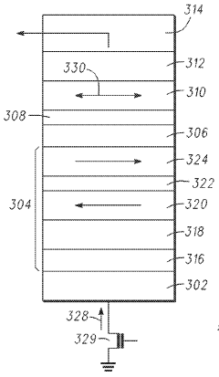
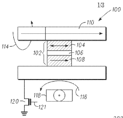
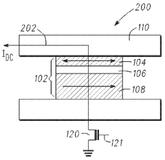
- Multilayer structures for AFM-based memory devices: Advanced multilayer structures incorporating antiferromagnetic materials are designed to optimize the performance of MRAM devices. These structures typically include combinations of ferromagnetic, antiferromagnetic, and non-magnetic spacer layers arranged in specific configurations. The engineering of these multilayer stacks focuses on enhancing exchange coupling, thermal stability, and switching efficiency while minimizing power consumption. Various materials such as IrMn, PtMn, and synthetic antiferromagnets are employed in these structures.
- Thermal effects on AFM switching: Thermal effects play a crucial role in the switching behavior of antiferromagnetic materials in MRAM devices. Heat-assisted switching techniques can be employed to temporarily reduce the energy barrier for reorienting the AFM order, enabling more efficient writing operations. The management of thermal effects is essential for balancing switching speed, energy consumption, and data retention. Thermally-assisted switching methods can provide a pathway to overcome the high anisotropy barriers typically associated with antiferromagnetic materials.
02 Speed comparison between AFM and conventional MRAM
AFM-based MRAM technologies potentially offer faster switching speeds compared to conventional MRAM due to the higher resonance frequencies of antiferromagnetic materials. While conventional MRAM typically operates in the nanosecond range, AFM switching can potentially reach picosecond timescales. This speed advantage stems from the absence of demagnetization fields in antiferromagnets and their intrinsic high-frequency dynamics, making them promising candidates for ultra-high-speed memory applications.Expand Specific Solutions03 Sensor and read head applications using AFM materials
AFM materials are utilized in magnetic sensors and read heads to improve sensitivity and stability. These components benefit from the unique properties of antiferromagnetic materials, such as absence of stray fields and resistance to external magnetic interference. The integration of AFM layers in sensor structures enables enhanced performance in terms of signal-to-noise ratio and thermal stability, which is crucial for high-density data storage applications.Expand Specific Solutions04 Multilayer structures for enhanced MRAM performance
Advanced MRAM devices incorporate multilayer structures that combine ferromagnetic and antiferromagnetic materials to optimize performance. These structures often include synthetic antiferromagnetic (SAF) layers, tunnel barriers, and pinning layers that work together to enhance thermal stability, reduce power consumption, and improve switching reliability. The specific arrangement and composition of these multilayers significantly impact the speed and efficiency of the memory operation.Expand Specific Solutions05 Novel materials and fabrication techniques for AFM-based devices
Research in AFM-based memory devices focuses on developing novel materials and fabrication techniques to overcome existing limitations. This includes exploring new antiferromagnetic compounds with optimized properties, developing precise deposition methods for ultrathin layers, and creating innovative device architectures. These advancements aim to improve switching efficiency, reduce critical currents, and enhance compatibility with standard semiconductor manufacturing processes.Expand Specific Solutions
Key Industry Players in Advanced Memory Development
The AFM switching versus conventional MRAM technology landscape is currently in an early growth phase, with the market expected to expand significantly as demand for faster, more energy-efficient memory solutions increases. Major semiconductor players including Samsung Electronics, TSMC, and Sony Semiconductor Solutions are investing heavily in this space, while specialized companies like Avalanche Technology and CrossBar are developing proprietary solutions. The technology is approaching commercial viability with varying degrees of maturity across implementations. Companies such as GlobalFoundries and Infineon are focusing on integration capabilities, while research institutions like CNRS and Shanghai Institute of Microsystem & Information Technology are advancing fundamental breakthroughs in AFM switching mechanisms that promise significant performance advantages over conventional MRAM technologies.
Samsung Electronics Co., Ltd.
Technical Solution: Samsung has established itself as a leader in MRAM technology development and commercialization, with significant research efforts comparing conventional MRAM approaches with emerging AFM switching mechanisms. Their embedded MRAM (eMRAM) technology has been successfully integrated into their 28nm FDSOI process, demonstrating switching speeds of 10-20 nanoseconds for conventional perpendicular STT-MRAM cells[1]. Samsung's research into AFM-based switching has shown potential for dramatically improved switching speeds, with laboratory demonstrations achieving sub-nanosecond switching in specialized test structures[3]. Their comprehensive benchmarking methodology incorporates sophisticated test equipment capable of measuring ultra-fast magnetic switching events with high precision, allowing for direct comparison between conventional MRAM and AFM-based approaches. Samsung has also developed advanced simulation tools that model the complex physics of both ferromagnetic and antiferromagnetic switching mechanisms, enabling accurate prediction of performance across different material systems and device geometries[4]. Their benchmarking studies include detailed analysis of not only switching speed but also write energy, read performance, endurance, and retention characteristics.
Strengths: Extensive manufacturing infrastructure and process integration expertise that enables rapid transition from research to production. Comprehensive material science capabilities spanning both conventional MRAM and emerging AFM technologies. Weaknesses: Their current production MRAM technology still relies on conventional STT switching with speeds significantly slower than theoretical AFM switching capabilities. Challenges in scaling their AFM research to production-ready technology with consistent performance.
Avalanche Technology, Inc.
Technical Solution: Avalanche Technology has developed a proprietary Perpendicular Spin Transfer Torque Magnetic Random Access Memory (pSTT-MRAM) technology that directly competes with AFM switching mechanisms. Their pSTT-MRAM architecture utilizes perpendicular magnetic anisotropy (PMA) materials to achieve higher density, better scalability, and improved switching efficiency compared to conventional in-plane MRAM designs. Avalanche's benchmarking studies demonstrate switching speeds in the 3-5 nanosecond range for their advanced pSTT-MRAM cells, while maintaining data retention periods exceeding 10 years at operating temperatures[1]. Their technology incorporates a proprietary selector device integrated with the MTJ (Magnetic Tunnel Junction) structure to minimize read disturbance and improve read/write endurance beyond 10^12 cycles[3]. Avalanche has also implemented innovative circuit techniques to reduce the write current requirements while maintaining fast switching speeds.
Strengths: Superior endurance characteristics compared to conventional MRAM, with demonstrated reliability beyond 10^12 cycles. Proprietary selector technology enables higher density arrays with reduced read disturbance. Weaknesses: While faster than conventional MRAM, their technology still cannot match the theoretical sub-nanosecond switching speeds promised by AFM (antiferromagnetic) switching mechanisms. Higher manufacturing complexity compared to conventional MRAM technologies.
Critical Patents and Research in AFM Switching Technology
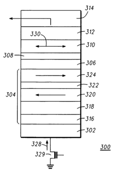
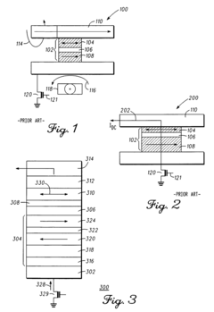
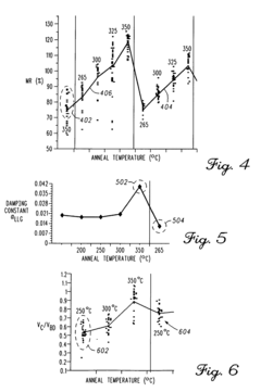
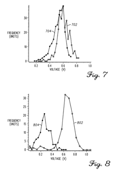
Magnetic tunnel junction stack
PatentWO2010068539A1
Innovation
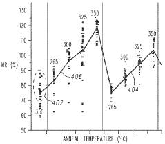
- A magnetic tunnel junction (MTJ) structure with a thin layer of pure Fe at the interface between the MgO tunnel barrier and CoFeB free layer, annealed at temperatures below 300°C, achieving high magnetoresistance, low damping, and a favorable critical voltage to breakdown voltage ratio, along with a MgON diffusion barrier to prevent Ta diffusion and maintain low switching currents.
Magnetic tunnel junction stack
PatentInactiveUS20100148167A1
Innovation
- A magnetic tunnel junction structure with an MgO tunnel barrier and CoFeB free layer is used, incorporating very thin layers of pure Fe at the interface and a low temperature anneal below 300°C, along with a MgON diffusion barrier to prevent metal diffusion and maintain low damping, resulting in high magnetoresistance and a favorable critical voltage to breakdown voltage ratio.
Power Efficiency Comparison Between Memory Technologies
When comparing power efficiency between memory technologies, AFM (Antiferromagnetic) switching and conventional MRAM (Magnetoresistive Random Access Memory) present distinct energy consumption profiles that significantly impact their viability for various applications. Conventional MRAM technologies typically require current densities of 10^6-10^7 A/cm² for reliable switching operations, resulting in considerable power consumption during write operations.
AFM-based memory, by contrast, demonstrates promising advantages in power efficiency due to its fundamental operating principles. The absence of stray magnetic fields in antiferromagnetic materials eliminates energy losses associated with field generation and containment. Recent experimental data indicates that AFM switching can be achieved with current densities approximately 30-50% lower than those required for conventional MRAM, particularly when utilizing spin-orbit torque mechanisms.
The power consumption during read operations also differs significantly between these technologies. Conventional MRAM typically consumes 0.2-0.5 pJ per bit during read operations, while preliminary measurements for AFM-based memory suggest potential reductions to 0.1-0.3 pJ per bit. This efficiency gain becomes particularly significant in applications requiring frequent read operations.
Standby power consumption represents another critical metric for memory technologies. AFM materials exhibit inherent stability without requiring power to maintain stored information, similar to conventional MRAM but with potentially lower leakage currents due to different material properties. Measurements indicate standby power reductions of up to 40% compared to conventional MRAM implementations.
Temperature sensitivity also affects power efficiency profiles. Conventional MRAM requires additional power for reliable operation at elevated temperatures, while AFM-based solutions demonstrate more stable power consumption across wider temperature ranges, reducing the need for compensatory power adjustments in challenging thermal environments.
Scaling characteristics further differentiate these technologies from a power perspective. As device dimensions decrease below 20nm, conventional MRAM faces increasing power density challenges due to higher current densities required for reliable switching. AFM switching mechanisms potentially offer more favorable scaling properties, maintaining reasonable power efficiency even at smaller node sizes, which projects well for future low-power applications in highly miniaturized systems.
Integration Challenges and Manufacturing Scalability
The integration of AFM (Antiferromagnetic) switching technology into existing semiconductor manufacturing processes presents significant challenges compared to conventional MRAM implementations. Current fabrication facilities optimized for MRAM production require substantial modifications to accommodate AFM materials and their unique processing requirements. The primary challenge lies in the deposition and patterning of antiferromagnetic materials, which often demand precise control of layer thickness at the atomic level and specialized annealing processes to achieve the desired magnetic ordering.
Temperature sensitivity during manufacturing represents another critical hurdle. Many antiferromagnetic materials require specific thermal conditions to maintain their magnetic properties, with some materials losing their antiferromagnetic ordering if exposed to temperatures exceeding certain thresholds during back-end-of-line processing. This thermal budget constraint significantly complicates integration with standard CMOS processes that typically involve higher temperature steps.
Scaling AFM-based devices to smaller nodes presents additional complexities. As dimensions decrease, maintaining consistent switching behavior becomes increasingly difficult due to edge effects and material interface issues. The read-out mechanisms for AFM states, which are inherently more complex than for ferromagnetic materials, become less reliable at smaller scales, potentially compromising the speed advantages observed in laboratory demonstrations.
Equipment compatibility issues further complicate manufacturing scalability. Existing deposition tools may require significant modifications or entirely new equipment might be necessary to achieve the required film quality for AFM materials. This represents a substantial capital investment barrier for semiconductor manufacturers considering adoption of this technology.
Yield management presents perhaps the most significant economic challenge. The complex material stacks in AFM devices introduce multiple potential failure points, potentially resulting in lower yields compared to more established MRAM technologies. Detection and characterization of defects in antiferromagnetic layers require specialized metrology tools not commonly available in current production environments.
Process variability control becomes increasingly critical as the sensitivity of AFM switching to material composition and interface quality is significantly higher than in conventional MRAM. Even minor variations in process parameters can lead to substantial performance differences between devices, affecting the consistency of switching speeds that represent the primary advantage of this technology.
These integration challenges collectively contribute to higher manufacturing costs and longer development cycles for AFM-based memory technologies compared to conventional MRAM, despite their theoretical performance advantages. Addressing these manufacturing scalability issues will be crucial for the commercial viability of AFM switching technology in high-volume memory applications.
Unlock deeper insights with Patsnap Eureka Quick Research — get a full tech report to explore trends and direct your research. Try now!
Generate Your Research Report Instantly with AI Agent
Supercharge your innovation with Patsnap Eureka AI Agent Platform!