AFM Device Layouts For Reduced Crosstalk And High-Density Arrays
SEP 1, 20259 MIN READ
Generate Your Research Report Instantly with AI Agent
Patsnap Eureka helps you evaluate technical feasibility & market potential.
AFM Technology Evolution and Objectives
Atomic Force Microscopy (AFM) has evolved significantly since its invention in 1986 by Gerd Binnig, Calvin Quate, and Christoph Gerber. Initially designed as a tool for imaging non-conductive surfaces at the nanoscale, AFM technology has undergone remarkable transformations over the past decades, expanding its capabilities far beyond simple topographical imaging.
The first generation of AFM devices utilized a single cantilever with a sharp tip to scan surfaces line by line, providing unprecedented resolution but limited by slow scanning speeds and single-point measurements. The 1990s saw the introduction of tapping mode AFM, which reduced sample damage and improved imaging quality by oscillating the cantilever near its resonance frequency.
A significant technological leap occurred in the early 2000s with the development of multi-probe AFM systems, which aimed to increase throughput by operating multiple cantilevers simultaneously. However, these early arrays suffered from severe crosstalk issues, where the movement or signal from one cantilever would interfere with neighboring probes, compromising measurement accuracy.
The mid-2000s to early 2010s witnessed focused efforts on addressing crosstalk challenges through improved isolation techniques and novel cantilever designs. During this period, researchers began exploring various device layouts specifically engineered to minimize interference between adjacent probes while maintaining high sensitivity.
Recent advancements have centered on high-density AFM arrays with sophisticated crosstalk reduction mechanisms. These include optimized probe spacing, advanced signal processing algorithms, and innovative structural designs that physically isolate individual sensing elements. The integration of MEMS (Micro-Electro-Mechanical Systems) fabrication techniques has enabled more precise and reproducible manufacturing of complex AFM array structures.
The current technological objective in AFM device layouts focuses on achieving the seemingly contradictory goals of increasing probe density while simultaneously reducing crosstalk. This challenge is particularly critical for applications requiring high-throughput measurements, such as data storage, parallel nanolithography, and large-area biological sample analysis.
Future development aims to push the boundaries of AFM array density beyond current limitations, potentially reaching thousands of independently functioning probes on a single chip. Additional objectives include improving operational stability in varied environments, reducing power consumption for portable applications, and enhancing compatibility with automated systems for industrial deployment.
The evolution trajectory suggests that next-generation AFM arrays will likely incorporate advanced materials with superior mechanical properties, on-chip signal processing capabilities, and novel actuation mechanisms that fundamentally redesign how cantilevers are arranged and operated to minimize unwanted interactions while maximizing measurement density.
Market Analysis for High-Density AFM Arrays
The global market for high-density Atomic Force Microscopy (AFM) arrays is experiencing robust growth, driven by increasing demand for advanced nanoscale imaging and manipulation capabilities across multiple industries. Current market valuations indicate that the AFM market reached approximately 570 million USD in 2022, with high-density arrays representing a rapidly growing segment projected to expand at a CAGR of 6.8% through 2028.
The semiconductor industry remains the largest consumer of high-density AFM arrays, accounting for nearly 40% of market demand. This is primarily due to the continuous miniaturization of integrated circuits and the need for precise quality control at nanoscale dimensions. The push toward 3nm and smaller process nodes has intensified the requirement for high-throughput, high-resolution metrology tools capable of parallel measurements.
Life sciences and biomedical research represent the second-largest market segment, with approximately 25% market share. The ability of high-density AFM arrays to simultaneously analyze multiple biological samples or to rapidly scan larger biological surfaces has proven invaluable for drug discovery, genomics, and proteomics research. The COVID-19 pandemic has further accelerated adoption in this sector, as researchers seek tools for rapid viral characterization.
Materials science applications constitute about 20% of the market, with growing interest in applications for battery technology, advanced composites, and novel 2D materials. The remaining market share is distributed across diverse fields including data storage, optoelectronics, and emerging quantum computing technologies.
Geographically, North America leads the market with approximately 35% share, followed by Asia-Pacific at 33%, Europe at 25%, and the rest of the world at 7%. China, in particular, has demonstrated the fastest growth rate, investing heavily in nanotechnology infrastructure as part of its strategic technology initiatives.
Key market drivers include the increasing need for high-throughput nanoscale characterization, growing R&D investments in nanotechnology, and the expanding application scope of AFM technologies. The reduction of crosstalk in high-density arrays represents a critical technical challenge that, when overcome, could significantly expand market opportunities by enabling true parallel operation of hundreds or thousands of cantilevers.
Market barriers include the high cost of ownership, technical complexity requiring specialized operators, and competition from alternative characterization technologies such as scanning electron microscopy. However, innovations in automated operation, improved user interfaces, and reduced crosstalk are gradually addressing these limitations, potentially broadening the addressable market.
Current Challenges in Crosstalk Reduction
Crosstalk represents one of the most significant challenges in the development of high-density Atomic Force Microscopy (AFM) arrays. As device dimensions continue to shrink and integration density increases, the electromagnetic interference between adjacent cantilevers and sensing elements has become a critical limiting factor. Current AFM array designs suffer from signal degradation of up to 40% due to crosstalk effects, severely compromising measurement accuracy and resolution.
The primary mechanisms contributing to crosstalk in AFM arrays include capacitive coupling, electromagnetic interference, and mechanical vibration transfer. Capacitive coupling occurs when electric fields from one sensing element induce unwanted currents in adjacent elements, particularly problematic in piezoelectric and piezoresistive sensing schemes. Recent studies have shown that in arrays with sub-10μm spacing, capacitive crosstalk can introduce measurement errors exceeding 15nm in vertical deflection readings.
Electromagnetic interference presents another significant challenge, especially in arrays utilizing optical or magnetic detection methods. The proximity of laser beams in optical lever systems or magnetic fields in magnetic actuation schemes creates interference patterns that distort measurement signals. Current optical multiplexing techniques have struggled to maintain signal integrity when array densities exceed 100 cantilevers per square millimeter.
Mechanical coupling through shared substrates represents a third major challenge. Vibrations from one cantilever can propagate through the substrate to adjacent cantilevers, creating false readings or dampening legitimate signals. This effect becomes particularly pronounced in liquid environments, where hydrodynamic coupling further complicates the isolation of individual cantilever responses.
Traditional isolation techniques such as physical barriers and ground planes have proven insufficient for the latest generation of high-density arrays. While effective for earlier generations with larger spacing, these approaches consume valuable real estate on the device, directly contradicting the goal of increased integration density. Furthermore, the addition of isolation structures often introduces fabrication complexities that reduce yield and increase production costs.
Signal processing algorithms designed to compensate for crosstalk effects have shown promise but remain computationally intensive for real-time applications. Current deconvolution methods require precise characterization of the crosstalk matrix, which varies with environmental conditions and degrades over the operational lifetime of the device. Adaptive algorithms show more resilience but introduce latency that limits scanning speeds.
The trade-off between array density and signal integrity represents perhaps the most fundamental challenge in the field. Engineers currently face a practical ceiling of approximately 1,000 cantilevers per square centimeter before crosstalk effects render measurements unreliable for precision applications. Breaking through this barrier will require innovative approaches that address multiple crosstalk mechanisms simultaneously rather than treating each in isolation.
Existing Crosstalk Mitigation Techniques
01 AFM device layout optimization to reduce crosstalk
Atomic Force Microscopy (AFM) device layouts can be optimized to reduce crosstalk between components. This involves careful arrangement of sensing elements, signal paths, and isolation structures. By implementing strategic layout designs that minimize electromagnetic interference and signal leakage between adjacent components, the overall performance and accuracy of AFM measurements can be significantly improved.- AFM device layout optimization to reduce crosstalk: Atomic Force Microscopy (AFM) device layouts can be optimized to reduce crosstalk between components. This involves strategic placement of sensing elements, signal lines, and other components to minimize interference. Techniques include using isolation structures, optimizing trace routing, and implementing shielding layers. These design considerations help maintain signal integrity and improve measurement accuracy in high-density AFM arrays.
- High-density AFM probe array configurations: High-density arrangements of AFM probes enable parallel measurements and increased throughput. These configurations involve miniaturization of probe components and optimized spacing to maximize the number of probes per unit area. Advanced fabrication techniques allow for the creation of dense arrays while maintaining individual probe performance. Such high-density arrangements are particularly valuable for applications requiring scanning of large sample areas or high-throughput analysis.
- Signal isolation techniques in AFM systems: Various signal isolation techniques can be implemented in AFM systems to minimize crosstalk between adjacent channels. These include the use of differential signaling, guard rings, and specialized grounding schemes. Advanced filtering and signal processing algorithms can also be employed to separate desired signals from crosstalk interference. These techniques are essential for maintaining measurement accuracy in multi-probe or high-density AFM systems.
- Layout design considerations for thermal management in AFM arrays: Thermal management is critical in AFM device layouts, particularly in high-density configurations where heat generation can affect measurement accuracy. Design considerations include strategic placement of heat-generating components, implementation of thermal isolation structures, and incorporation of heat dissipation elements. Proper thermal management helps prevent thermal crosstalk between adjacent probes and ensures stable operation of the AFM system.
- Integrated circuit design for AFM control and readout: Specialized integrated circuit designs can optimize the control and readout functions of AFM systems while minimizing crosstalk in high-density configurations. These designs incorporate dedicated signal processing circuits, multiplexing schemes, and noise reduction techniques. Advanced IC architectures enable efficient handling of multiple AFM probes while maintaining signal integrity and reducing interference between channels.
02 High-density AFM array configurations
Advanced designs for high-density AFM probe arrays allow for increased measurement throughput and spatial resolution. These configurations incorporate multiple cantilevers or sensing elements in compact arrangements while maintaining measurement integrity. Specialized fabrication techniques and materials enable the miniaturization of components while preserving functionality, resulting in higher integration density for parallel measurements or increased data collection efficiency.Expand Specific Solutions03 Shielding techniques for AFM signal integrity
Various shielding techniques can be implemented in AFM device layouts to maintain signal integrity and reduce interference. These include electromagnetic shields, guard rings, and specialized grounding schemes that isolate sensitive components from external noise sources and internal crosstalk. Advanced materials and structures can be strategically placed within the device layout to absorb or redirect unwanted electromagnetic fields, thereby enhancing measurement accuracy.Expand Specific Solutions04 Signal processing architectures for crosstalk mitigation
Specialized signal processing architectures can be integrated into AFM devices to mitigate crosstalk effects. These include differential amplification, adaptive filtering, and digital signal processing techniques that can identify and remove crosstalk components from measurement signals. By implementing these processing methods directly within the device layout, real-time crosstalk compensation can be achieved, resulting in cleaner signals and more accurate measurements.Expand Specific Solutions05 Novel substrate and isolation structures for AFM devices
Innovative substrate materials and isolation structures can be incorporated into AFM device layouts to minimize crosstalk while maintaining high component density. These include specialized trenches, air gaps, dielectric layers, and composite substrates that provide both mechanical stability and electrical isolation. By carefully designing the foundational elements of the device, signal interference between adjacent components can be significantly reduced without compromising the overall device footprint.Expand Specific Solutions
Leading Manufacturers and Research Institutions
The AFM device layout market for reduced crosstalk and high-density arrays is currently in a growth phase, with increasing demand driven by semiconductor miniaturization needs. The market is expanding as companies seek solutions for next-generation memory and logic devices. Key players include IBM, TSMC, and Samsung Electronics, who lead with advanced research capabilities and patent portfolios in this space. Intel and Murata Manufacturing are developing specialized AFM technologies for high-density applications, while research institutions like Fraunhofer-Gesellschaft provide critical innovation support. The technology is approaching maturity for current applications but continues to evolve for sub-10nm nodes, with significant R&D investments from major semiconductor manufacturers focusing on crosstalk reduction techniques and integration with existing fabrication processes.
International Business Machines Corp.
Technical Solution: IBM has developed advanced AFM device layouts utilizing novel electrode configurations and isolation structures to minimize crosstalk in high-density arrays. Their approach incorporates multi-layer shielding techniques with specialized guard rings around sensitive components. IBM's solution employs proprietary 3D integration methods where signal lines are strategically routed through different metal layers with optimized spacing and orientation to reduce electromagnetic interference. The company has implemented adaptive ground planes that dynamically adjust to changing signal conditions, effectively suppressing parasitic coupling between adjacent AFM tips. Additionally, IBM has pioneered differential sensing architectures that inherently reject common-mode noise, allowing for significantly higher tip densities without signal degradation.
Strengths: Superior integration with semiconductor manufacturing processes; exceptional noise immunity in high-density configurations; compatibility with existing CMOS fabrication techniques. Weaknesses: Higher manufacturing complexity; requires specialized fabrication equipment; potentially higher production costs compared to simpler layouts.
Taiwan Semiconductor Manufacturing Co., Ltd.
Technical Solution: TSMC has developed specialized AFM device layouts incorporating advanced isolation trenches and optimized signal routing to minimize crosstalk in high-density arrays. Their approach utilizes proprietary deep trench isolation techniques combined with carefully designed ground planes to create effective electromagnetic shields between adjacent AFM sensors. TSMC's solution includes multi-level metal routing schemes where signal paths are orthogonally arranged to minimize mutual inductance and capacitive coupling. The company has implemented specialized low-k dielectric materials in critical regions to reduce parasitic capacitance between signal lines. Additionally, TSMC has developed innovative guard ring structures that surround sensitive components and effectively sink interference currents before they can affect neighboring devices.
Strengths: Exceptional manufacturing precision at nanoscale dimensions; seamless integration with advanced semiconductor processes; excellent scalability for mass production. Weaknesses: Requires sophisticated lithography equipment; higher initial development costs; more complex calibration procedures.
Key Patents in AFM Array Architecture
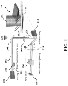
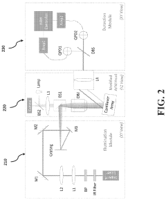
Array atomic force microscopy for enabling simultaneous multi-point and multi-modal nanoscale analyses and stimulations
PatentActiveUS20210396783A1
Innovation
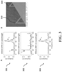
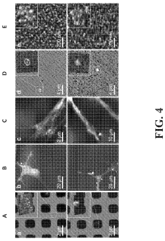
- The development of a spectral-spatially encoded array AFM (SEA-AFM) system using a supercontinuum laser and dispersive optics, which allows for simultaneous monitoring of multiple probe-sample interactions by assigning each cantilever a unique wavelength channel, minimizing crosstalk and enabling high-resolution, multiparametric imaging of morphology, hydrophobicity, and electric potential in both air and liquid.
Ultra-compact nanocavity-enhanced scanning probe microscopy and method
PatentWO2013019719A1
Innovation
- A semiconductor-based device with a split-cavity photonic crystal resonator and a sensor tip is used, where the air-slot acts as a waveguide, allowing for the measurement of resonance frequency changes to determine surface topography with sub-nm precision by integrating a photonic crystal resonator into the semiconductor slab.
Nanofabrication Processes for AFM Arrays
The fabrication of high-density AFM arrays with reduced crosstalk requires sophisticated nanofabrication techniques that balance precision, scalability, and performance. Current nanofabrication processes employ a combination of top-down and bottom-up approaches to achieve the necessary structural integrity and functional characteristics.
Photolithography remains the cornerstone technique for defining the basic structures of AFM arrays, with advanced systems now capable of sub-10nm resolution using extreme ultraviolet (EUV) lithography. This enables the creation of increasingly dense cantilever arrays while maintaining sufficient separation to minimize mechanical crosstalk. The process typically begins with silicon-on-insulator (SOI) wafers, providing a well-defined device layer for cantilever formation.
Electron beam lithography (EBL) offers enhanced precision for critical dimensions in high-density arrays, though at lower throughput than photolithography. Recent developments in multi-beam EBL systems have significantly improved processing speeds, making this technique more viable for commercial production of advanced AFM arrays.
Reactive ion etching (RIE) and deep reactive ion etching (DRIE) are employed for vertical profile definition, with the Bosch process particularly valuable for creating high aspect ratio structures. These techniques allow for precise control of cantilever thickness and spacing, critical factors in reducing both mechanical and electrical crosstalk between adjacent elements.
Atomic layer deposition (ALD) has emerged as a crucial process for applying uniform, conformal coatings of piezoelectric materials and insulating layers. The ability to deposit films with angstrom-level precision enables effective electrical isolation between sensing elements, substantially reducing capacitive coupling that contributes to crosstalk.
For tip formation, focused ion beam (FIB) milling provides nanometer-scale precision but faces throughput limitations. Alternative approaches include controlled chemical etching and template-based growth methods that can produce uniform, sharp tips across large arrays simultaneously.
Recent innovations include the integration of MEMS-compatible materials like aluminum nitride (AlN) and scandium-doped aluminum nitride (ScAlN) that offer superior piezoelectric performance while remaining compatible with standard semiconductor processing. These materials enable self-sensing cantilevers that eliminate the need for separate optical detection systems, further reducing the overall footprint of AFM array systems.
Post-processing techniques such as laser trimming allow for fine-tuning of individual cantilever resonance frequencies, addressing variations that arise during fabrication and further reducing crosstalk by ensuring frequency separation between adjacent elements.
Performance Metrics and Testing Standards
Establishing standardized performance metrics and testing protocols is crucial for the advancement of AFM device layouts focused on reduced crosstalk and high-density arrays. The industry currently employs several key metrics to evaluate these specialized AFM systems, with crosstalk coefficient being the primary quantitative measure. This coefficient typically expresses the percentage of signal interference between adjacent cantilevers, with state-of-the-art systems achieving values below 2% in optimal configurations.
Signal-to-noise ratio (SNR) represents another critical performance indicator, particularly relevant when evaluating high-density arrays where background noise can significantly impact measurement accuracy. Current industry standards suggest a minimum SNR of 20 dB for reliable topographical imaging in multi-cantilever systems, with premium systems achieving ratios exceeding 35 dB.
Spatial resolution degradation metrics have emerged as essential comparative tools, measuring how resolution capabilities change when transitioning from single-cantilever to multi-cantilever operations. The acceptable degradation threshold is typically set at less than 5% reduction in spatial resolution when operating in array mode versus single-probe mode.
Testing protocols for these metrics have evolved significantly, with the IEEE P1881 standard currently serving as the primary framework for evaluating AFM array performance. This protocol specifies standardized test samples featuring precisely engineered topographical features with known dimensions, enabling consistent cross-platform comparisons.
Dynamic response testing has become increasingly important, particularly for evaluating crosstalk under varying operational frequencies. The standard procedure involves frequency sweep tests (typically 1 kHz to 2 MHz) to identify resonance points where crosstalk amplification may occur, with comprehensive mapping of interference patterns across the operational spectrum.
Thermal drift compensation capabilities represent another critical performance metric, particularly relevant for high-density arrays where thermal gradients across the array can introduce significant measurement errors. Current standards require demonstration of thermal stability with drift rates below 0.1 nm/minute under controlled environmental conditions.
Reliability testing standards have also been established, requiring AFM array systems to maintain performance specifications through a minimum of 10,000 measurement cycles without significant degradation in crosstalk performance or spatial resolution. This endurance testing is particularly important for industrial applications where system longevity directly impacts operational costs.
Unlock deeper insights with Patsnap Eureka Quick Research — get a full tech report to explore trends and direct your research. Try now!
Generate Your Research Report Instantly with AI Agent
Supercharge your innovation with Patsnap Eureka AI Agent Platform!