Integration Strategies For Antiferromagnetic Layers With CMOS Back-End
SEP 1, 20259 MIN READ
Generate Your Research Report Instantly with AI Agent
Patsnap Eureka helps you evaluate technical feasibility & market potential.
AFM-CMOS Integration Background and Objectives
Antiferromagnetic (AFM) materials have emerged as promising candidates for next-generation spintronic devices due to their unique properties including zero net magnetization, robustness against external magnetic field perturbations, and ultrafast dynamics in the terahertz range. The integration of AFM layers with complementary metal-oxide-semiconductor (CMOS) back-end processes represents a critical technological frontier that could revolutionize computing architectures by enabling novel memory and logic functionalities.
The evolution of spintronics has progressed from giant magnetoresistance (GMR) to tunneling magnetoresistance (TMR) effects, with ferromagnetic materials traditionally dominating the field. However, the limitations of ferromagnetic-based devices, particularly in terms of scaling and energy efficiency, have driven research toward antiferromagnetic materials as alternative building blocks for spintronic applications.
The primary objective of AFM-CMOS integration is to develop scalable, energy-efficient computing elements that leverage the intrinsic advantages of antiferromagnetic materials while maintaining compatibility with established semiconductor manufacturing processes. This integration aims to address the growing challenges of power consumption and heat dissipation in conventional CMOS technologies, which are approaching fundamental physical limits.
From a historical perspective, the practical utilization of antiferromagnetic materials has been hindered by difficulties in detecting and manipulating their magnetic order. Recent breakthroughs in electrical reading and writing of antiferromagnetic states, particularly through spin-orbit torque mechanisms, have revitalized interest in these materials for practical applications.
The technological trajectory indicates a convergence of two previously distinct domains: antiferromagnetic spintronics and silicon-based microelectronics. This convergence necessitates overcoming significant materials science and process engineering challenges, including thermal budget constraints, interface quality control, and structural compatibility between AFM layers and CMOS back-end materials.
Key technological goals include developing reliable deposition methods for high-quality AFM thin films at CMOS-compatible temperatures, establishing robust electrical contacts between AFM elements and CMOS interconnects, and designing circuit architectures that effectively harness the unique properties of antiferromagnetic materials.
The long-term vision encompasses creating hybrid computing systems that combine the processing capabilities of CMOS with the non-volatile, high-speed characteristics of AFM-based memory and logic elements. Such integration could potentially enable novel computing paradigms, including neuromorphic architectures and in-memory computing, which are particularly suited for emerging artificial intelligence applications.
Market Analysis for AFM-CMOS Integrated Devices
The integration of antiferromagnetic (AFM) materials with CMOS back-end technology represents a significant market opportunity across multiple sectors. Current market projections indicate that the global spintronics market, which encompasses AFM-CMOS integrated devices, is expected to grow at a compound annual growth rate of 34% through 2028, reaching approximately $5.2 billion.
The primary market drivers for AFM-CMOS integrated devices stem from increasing demands for non-volatile memory solutions with enhanced performance characteristics. Traditional MRAM technologies based on ferromagnetic materials face scaling limitations that AFM-based alternatives can potentially overcome, creating substantial market pull from memory manufacturers seeking next-generation solutions.
Data center applications represent the largest immediate market opportunity, with server manufacturers actively seeking memory technologies that combine the speed of SRAM with the non-volatility of flash memory, while significantly reducing power consumption. AFM-CMOS integrated devices could potentially reduce data center energy consumption by up to 25% when implemented in memory hierarchies.
The automotive sector presents another substantial growth vector, particularly with the rise of electric and autonomous vehicles requiring radiation-hardened, temperature-stable memory solutions. Market research indicates that automotive-grade memory requirements will increase threefold by 2026, creating a specialized niche where AFM-CMOS technologies hold competitive advantages.
Consumer electronics manufacturers are also showing interest in AFM-CMOS integration for mobile devices, where power efficiency and form factor are critical considerations. The ability to create normally-off computing architectures could extend battery life by 30-40% in smartphones and wearable devices.
Industrial IoT applications represent an emerging market segment with significant growth potential. The need for edge computing devices that can operate in harsh environments with minimal power requirements aligns perfectly with the capabilities of AFM-CMOS integrated solutions.
Market barriers include competition from established memory technologies with mature ecosystems, manufacturing scalability challenges, and the current cost premium associated with novel materials integration. Industry analysts estimate that AFM-CMOS solutions must achieve a cost reduction of approximately 40% to become competitive with incumbent technologies in mainstream applications.
Regional market analysis reveals that North America and Asia-Pacific currently lead in research and development investments, with major semiconductor manufacturers in Taiwan, South Korea, and the United States establishing strategic partnerships with materials science companies to accelerate commercialization timelines.
AFM Integration Challenges and Technical Barriers
The integration of antiferromagnetic (AFM) layers with CMOS back-end processes presents significant technical challenges that must be addressed for successful commercialization. The primary barrier stems from the thermal budget constraints of CMOS back-end-of-line (BEOL) processing, which typically limits temperatures to below 400°C. Many high-quality AFM materials require deposition or annealing temperatures exceeding this threshold, creating a fundamental compatibility issue.
Material selection represents another critical challenge. Ideal AFM materials must simultaneously satisfy multiple requirements: CMOS compatibility, appropriate blocking temperature, suitable exchange bias properties, and long-term stability. Materials such as IrMn and PtMn offer promising properties but present integration difficulties due to their complex deposition requirements and potential for diffusion into adjacent layers.
Deposition technique optimization presents significant hurdles. Conventional methods like sputtering can induce damage to underlying CMOS structures through ion bombardment, while techniques like atomic layer deposition (ALD) may not achieve the crystalline quality necessary for optimal AFM performance. The industry lacks standardized deposition protocols specifically tailored for AFM integration with CMOS.
Interface engineering between AFM layers and adjacent materials constitutes another major technical barrier. The exchange coupling at these interfaces directly impacts device performance, yet controlling atomic-level interactions during manufacturing remains challenging. Interdiffusion, oxidation, and interfacial roughness can significantly degrade the desired magnetic properties.
Dimensional scaling presents increasing difficulties as device sizes approach nanometer scales. AFM domain structures and grain boundaries become proportionally more significant at reduced dimensions, potentially compromising performance consistency. Current lithography and etching techniques struggle to precisely pattern AFM materials without introducing edge damage that affects magnetic properties.
Characterization and testing methodologies for integrated AFM-CMOS structures remain underdeveloped. Conventional magnetic measurement techniques often lack the sensitivity required for thin-film AFM materials, particularly when embedded within complex device structures. This hampers both research progress and quality control in manufacturing environments.
Reliability and aging effects constitute a significant concern for commercial applications. AFM materials may experience performance degradation over time due to thermal cycling, electrical stress, or atomic diffusion. The industry lacks comprehensive long-term reliability data for AFM-CMOS integrated devices, creating uncertainty for product lifetime predictions.
Standardization across the industry represents a final major barrier. The absence of established integration protocols, material specifications, and testing methodologies impedes knowledge sharing and technology transfer between research institutions and commercial manufacturers, ultimately slowing industry-wide progress toward viable AFM-CMOS integrated technologies.
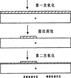
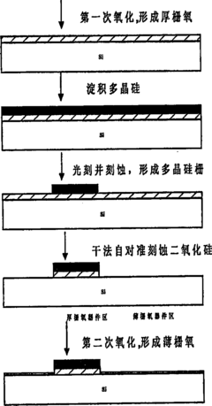
Current AFM-CMOS Back-End Integration Methods
01 Antiferromagnetic layer structure in magnetic read heads
Antiferromagnetic layers are integrated into magnetic read head structures to provide exchange bias for pinned magnetic layers. These structures typically include a stack of layers with specific thicknesses and compositions to optimize the exchange coupling and thermal stability. The integration of antiferromagnetic materials like IrMn, PtMn, or NiMn helps stabilize the magnetization direction of adjacent ferromagnetic layers, which is crucial for the proper functioning of magnetoresistive sensors in hard disk drives.- Antiferromagnetic layer structure in magnetic read heads: Antiferromagnetic layers are integrated into magnetic read head structures to provide exchange bias for pinned magnetic layers. These structures typically include a pinned ferromagnetic layer coupled to an antiferromagnetic layer, which stabilizes the magnetization direction of the pinned layer. This configuration enhances the stability and performance of magnetoresistive sensors used in hard disk drives, allowing for improved read sensitivity and signal-to-noise ratio.
- Materials selection for antiferromagnetic layers: Various materials are used for antiferromagnetic layers in magnetic devices, including PtMn, IrMn, NiMn, FeMn, and PdMn alloys. The selection of appropriate antiferromagnetic materials is critical for achieving desired exchange coupling strength, thermal stability, and corrosion resistance. Material composition and thickness are optimized to ensure proper pinning strength while maintaining compatibility with adjacent layers in the magnetic stack.
- Synthetic antiferromagnetic structures: Synthetic antiferromagnetic (SAF) structures consist of two ferromagnetic layers separated by a non-magnetic spacer layer, typically ruthenium. These structures provide enhanced stability through antiferromagnetic coupling between the ferromagnetic layers, reducing stray fields and improving device performance. SAF structures are integrated into various magnetic devices to achieve better thermal stability and reduced magnetostatic interactions.
- Antiferromagnetic layer integration in MRAM devices: In Magnetic Random Access Memory (MRAM) devices, antiferromagnetic layers are integrated to stabilize reference layers in magnetic tunnel junctions. The integration process involves careful control of deposition parameters, annealing conditions, and interface engineering to ensure strong exchange coupling and thermal stability. These antiferromagnetic layers help maintain the fixed magnetization direction of reference layers during write operations and under thermal fluctuations.
- Novel antiferromagnetic materials and structures: Recent advancements include the development of novel antiferromagnetic materials and structures with enhanced properties. These innovations include antiferromagnetic materials with higher blocking temperatures, reduced thickness requirements, and improved exchange coupling. Some approaches involve multilayer structures, doping strategies, and interface engineering to optimize the performance of antiferromagnetic layers in spintronic devices, potentially enabling new functionalities and applications.
02 Synthetic antiferromagnetic structures
Synthetic antiferromagnetic (SAF) structures consist of two ferromagnetic layers separated by a non-magnetic spacer layer, typically ruthenium. These structures are integrated into spintronic devices to create strong antiferromagnetic coupling between the ferromagnetic layers, resulting in improved thermal stability and reduced magnetostatic interactions. The thickness of the spacer layer is critical for controlling the strength and type of coupling between the ferromagnetic layers, allowing for customization of magnetic properties without using traditional antiferromagnetic materials.Expand Specific Solutions03 Antiferromagnetic layer deposition and patterning techniques
Various deposition and patterning techniques are employed for integrating antiferromagnetic layers into magnetic devices. These include magnetron sputtering, ion beam deposition, and molecular beam epitaxy, followed by lithographic patterning processes. The deposition conditions, such as substrate temperature, pressure, and post-deposition annealing, significantly affect the crystalline structure and exchange bias properties of the antiferromagnetic layers. Advanced patterning techniques allow for precise definition of antiferromagnetic regions in nanoscale devices.Expand Specific Solutions04 Antiferromagnetic materials for MRAM applications
Antiferromagnetic materials are integrated into Magnetic Random Access Memory (MRAM) devices to enhance thermal stability and data retention. The integration involves careful selection of antiferromagnetic materials with appropriate blocking temperatures and exchange bias strengths. These materials help pin the reference layer in magnetic tunnel junctions, allowing for reliable switching of the free layer during write operations while maintaining data stability during read operations. The thickness and composition of the antiferromagnetic layer are optimized to balance exchange bias strength with overall device performance.Expand Specific Solutions05 Interface engineering for enhanced exchange coupling
Interface engineering between antiferromagnetic and ferromagnetic layers is crucial for optimizing exchange coupling strength and thermal stability. Techniques include insertion of thin spacer layers, interface roughness control, and compositional grading at the interface. The atomic-scale structure at the interface significantly influences the exchange bias field and its temperature dependence. Advanced multilayer structures with engineered interfaces can achieve enhanced exchange coupling, improved blocking temperature, and reduced training effects, which are essential for high-performance spintronic devices operating at elevated temperatures.Expand Specific Solutions
Key Industry Players in AFM-CMOS Integration
The integration of antiferromagnetic layers with CMOS back-end technology is currently in an early growth phase, with the market expanding as spintronic applications gain traction. Major semiconductor players including IBM, TSMC, Samsung, and GlobalFoundries are advancing this field alongside specialized companies like Everspin Technologies. Research institutions such as Peking University, IMEC, and CEA are contributing significant innovations. The technology remains in development stages with varying maturity levels across applications. Industry leaders are focusing on overcoming integration challenges between antiferromagnetic materials and conventional CMOS processes, with particular progress in memory applications where companies like Micron and Western Digital are exploring commercial implementations.
International Business Machines Corp.
Technical Solution: IBM has developed a comprehensive integration strategy for antiferromagnetic (AFM) layers with CMOS back-end processes, focusing on spin-orbit torque magnetic random access memory (SOT-MRAM) devices. Their approach utilizes antiferromagnetic materials like PtMn and IrMn as both the spin current source and pinning layer in a single structure. IBM's process involves depositing AFM materials at temperatures compatible with CMOS back-end (below 400°C), followed by precise patterning using reactive ion etching techniques that preserve the magnetic properties. They've demonstrated successful integration of these AFM layers with standard 300mm CMOS wafers, achieving thermal stability up to 400°C without degradation of magnetic properties. IBM's technology enables switching currents below 100μA and switching speeds in the sub-nanosecond range, making it suitable for last-level cache applications in high-performance computing systems.
Strengths: IBM's approach offers excellent CMOS compatibility with their established semiconductor manufacturing infrastructure, enabling seamless integration into existing production lines. Their dual-function AFM layers (both as spin source and pinning layer) reduce stack complexity and process steps. Weaknesses: The technology requires precise control of AFM layer thickness and composition, which can lead to variability issues in high-volume manufacturing. The approach may also have higher power consumption compared to some competing technologies.
Taiwan Semiconductor Manufacturing Co., Ltd.
Technical Solution: TSMC has developed a comprehensive integration strategy for antiferromagnetic materials with their advanced CMOS back-end processes, focusing on embedded MRAM (eMRAM) applications. Their approach utilizes a "hybrid integration" technique where antiferromagnetic layers (primarily IrMn and PtMn) are incorporated into magnetic tunnel junction (MTJ) stacks using a specialized deposition sequence that maintains temperatures below 400°C throughout the process. TSMC's integration method involves a unique "damage-free patterning" approach that combines advanced lithography with selective etching techniques to precisely define the AFM-based MTJ structures while preserving their magnetic properties. They've successfully demonstrated this technology in their 22nm and 16nm FinFET process nodes, achieving switching currents below 100μA and write speeds under 10ns. TSMC's AFM-integrated devices show excellent thermal stability (data retention >10 years at 125°C) and endurance exceeding 10^12 cycles, making them suitable for automotive and industrial IoT applications. Their process achieves bit cell sizes below 0.04μm² in their 16nm node, enabling high-density integration for embedded applications.
Strengths: TSMC's established manufacturing infrastructure enables seamless integration into existing high-volume production lines with excellent yield control. Their damage-free patterning approach preserves magnetic properties better than conventional etching methods. Weaknesses: The technology currently faces challenges with scaling below 10nm due to limitations in controlling AFM domain structures at smaller dimensions. The specialized deposition and etching processes add manufacturing complexity and potential cost increases.
Critical Patents and Research in AFM-CMOS Integration
Technique for preparing dual-gate oxygen on CMOS in high voltage compatible to standard technique of CMOS
PatentInactiveCN1873954A
Innovation
- Using a dry-wet etching method, the polysilicon gate is self-aligned to etch the thick gate oxide, and the step height of the polysilicon gate and the thin gate oxide area is relaxed through regular etching and sidewalls, combined with hydrofluoric acid bleaching. Protect the silicon surface and form a dual-gate oxide preparation process that is compatible with standard CMOS processes.
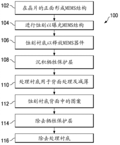
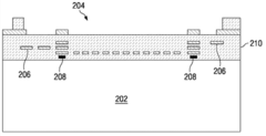
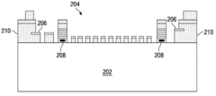
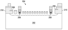
Method of fabricating an integrated CMOS-MEMS device
PatentInactiveCN102757015A
Innovation
- Using a sacrificial layer process, the MEMS mechanical structure is formed on the front side of the substrate, and the MEMS device is released in subsequent processing through sacrificial layer protection, reducing substrate processing, providing a buffer layer to reduce or eliminate over-etching, and finally releasing through dry etching and cleaning processes The active structure of MEMS devices.
Thermal Management Strategies for AFM-CMOS Systems
Thermal management represents a critical challenge in the integration of antiferromagnetic (AFM) layers with CMOS back-end processes. The temperature sensitivity of AFM materials combined with the heat generated during CMOS operation creates a complex thermal environment that must be carefully managed to ensure system reliability and performance.
Current thermal management approaches for AFM-CMOS systems employ multi-layered strategies. Thermal barrier layers composed of materials with low thermal conductivity, such as SiO2 or specialized polymers, are strategically placed between heat-generating components and temperature-sensitive AFM elements. These barriers effectively isolate the AFM layers from thermal fluctuations that could compromise their magnetic ordering.
Advanced heat sink designs represent another crucial component in thermal management frameworks. Copper-based heat spreaders with optimized geometries facilitate efficient heat dissipation away from critical junctions. Recent innovations include three-dimensional heat sink architectures that maximize surface area while minimizing the overall footprint, addressing the spatial constraints inherent in integrated circuit designs.
On-chip thermal sensors provide real-time temperature monitoring capabilities, enabling dynamic thermal management. These sensors, typically implemented as resistance temperature detectors (RTDs) or thermocouples, are strategically positioned near AFM-CMOS interfaces to detect localized hotspots. The data collected informs adaptive cooling mechanisms that respond to changing thermal conditions during operation.
Active cooling solutions, including micro-fluidic channels and thermoelectric coolers, offer more aggressive thermal management for high-performance applications. Micro-fluidic systems circulate coolants through channels etched directly into the substrate, providing targeted cooling to thermal hotspots. Thermoelectric coolers leverage the Peltier effect to transfer heat away from sensitive components, though their integration presents additional design challenges.
Thermal-aware circuit design techniques complement hardware solutions by optimizing power distribution and switching patterns to minimize heat generation. Dynamic frequency scaling and selective power gating reduce thermal loads during operation, while workload distribution algorithms prevent the formation of persistent hotspots by balancing computational tasks across the chip area.
Emerging approaches include phase-change materials that absorb thermal energy during state transitions, providing passive thermal buffering during transient temperature spikes. Additionally, graphene-based thermal interface materials show promise for next-generation thermal management due to their exceptional in-plane thermal conductivity and mechanical flexibility.
Scalability and Manufacturing Considerations
The integration of antiferromagnetic (AFM) layers with CMOS back-end processes presents significant scalability and manufacturing challenges that must be addressed for successful commercialization. As device dimensions continue to shrink following Moore's Law, maintaining the integrity and performance of AFM materials becomes increasingly difficult. Current manufacturing processes typically require temperatures below 400°C to ensure compatibility with CMOS back-end-of-line (BEOL) thermal budgets, limiting the selection of viable AFM materials and deposition techniques.
Deposition uniformity across large-diameter wafers (300mm and beyond) represents a critical manufacturing consideration. Techniques such as magnetron sputtering and atomic layer deposition (ALD) show promise for achieving the necessary thickness control at the nanometer scale, but process optimization remains challenging when transitioning from research to high-volume manufacturing environments. The industry must develop improved metrology tools capable of characterizing AFM layer properties in-line during production.
Etch selectivity and pattern transfer present additional manufacturing hurdles. Conventional plasma etching processes may induce damage to AFM layers, potentially altering their magnetic properties. Development of low-damage etching techniques with high selectivity between AFM materials and surrounding dielectrics or metals is essential for maintaining device performance. Advanced patterning approaches such as self-aligned double patterning (SADP) may be necessary to achieve the required feature dimensions.
Integration with existing CMOS fabrication lines requires careful consideration of contamination control. Many AFM materials contain elements not typically present in standard CMOS processes, raising concerns about cross-contamination. Dedicated equipment or specialized handling protocols may be necessary, potentially increasing manufacturing costs and complexity. The industry must establish appropriate contamination monitoring and control strategies.
Yield management represents perhaps the greatest scalability challenge. AFM-based devices are highly sensitive to process variations and defects, requiring tighter process control than conventional CMOS components. Statistical process control methodologies must be adapted to monitor the unique failure modes associated with AFM integration. Early involvement of yield engineering teams in technology development can help identify and mitigate potential manufacturing issues before high-volume production.
Cost considerations ultimately determine commercial viability. While AFM materials offer significant performance advantages, their integration must not substantially increase overall manufacturing costs. Process simplification, equipment sharing with existing CMOS steps, and material optimization are essential strategies for maintaining cost competitiveness. The industry should explore opportunities for equipment reuse and process consolidation to minimize the economic impact of AFM integration.
Unlock deeper insights with Patsnap Eureka Quick Research — get a full tech report to explore trends and direct your research. Try now!
Generate Your Research Report Instantly with AI Agent
Supercharge your innovation with Patsnap Eureka AI Agent Platform!