What Is Antiferromagnetic Spintronics And Why It Matters For Memory
SEP 1, 20259 MIN READ
Generate Your Research Report Instantly with AI Agent
Patsnap Eureka helps you evaluate technical feasibility & market potential.
Antiferromagnetic Spintronics Background and Objectives
Spintronics, a field that leverages both the spin and charge properties of electrons, has evolved significantly since its inception in the late 1980s. While conventional spintronics primarily utilizes ferromagnetic materials, antiferromagnetic (AFM) spintronics has emerged as a revolutionary branch with distinct advantages for next-generation memory technologies. The historical trajectory of AFM spintronics began with theoretical explorations in the early 2000s, followed by experimental breakthroughs around 2010-2015 that demonstrated electrical manipulation of antiferromagnetic order.
Antiferromagnetic materials possess unique characteristics that make them particularly attractive for memory applications. Unlike ferromagnets, AFM materials exhibit no net magnetic moment, making them inherently robust against external magnetic field disturbances. This intrinsic stability represents a significant advantage for data security and reliability in memory devices. Additionally, AFM materials typically operate at much higher frequencies (in the terahertz range) compared to ferromagnets, potentially enabling ultrafast memory operations.
The technological evolution of AFM spintronics has been marked by several pivotal discoveries, including the observation of anisotropic magnetoresistance in antiferromagnets, the demonstration of electrical switching of antiferromagnetic order, and the development of methods to read antiferromagnetic states. These advancements have collectively established the fundamental building blocks for AFM-based memory technologies.
Current research trends in this field are focused on overcoming key challenges such as efficient electrical control of antiferromagnetic order, reliable detection of AFM states, and integration with existing semiconductor technologies. The scientific community is particularly interested in exploring novel material systems, including synthetic antiferromagnets and antiferromagnetic topological insulators, which may offer enhanced performance characteristics.
The primary objectives of antiferromagnetic spintronics research for memory applications include developing energy-efficient writing mechanisms, enhancing readout signal magnitudes, improving thermal stability, and achieving compatibility with CMOS fabrication processes. These goals align with the broader industry demands for memory technologies that offer higher density, faster operation, lower power consumption, and improved reliability.
Looking forward, the field aims to transition from fundamental research to practical applications, with particular emphasis on creating viable prototypes of AFM-based memory devices. This includes addressing scalability issues and establishing standardized characterization methods for antiferromagnetic memory elements. The ultimate vision is to position AFM spintronics as a cornerstone technology for future computing architectures, potentially enabling novel computing paradigms beyond the traditional von Neumann approach.
Market Demand Analysis for Next-Generation Memory
The memory technology market is experiencing a significant transformation driven by the increasing demands of data-intensive applications. Current projections indicate the global next-generation memory market will reach approximately $20 billion by 2026, with a compound annual growth rate exceeding 29%. This growth is primarily fueled by the limitations of conventional memory technologies in meeting the requirements of emerging computing paradigms.
Antiferromagnetic spintronics represents a promising solution to address these market demands. Traditional memory technologies face fundamental challenges: DRAM requires constant power refreshing, SRAM consumes excessive chip area, and even current spintronic solutions like MRAM face scalability issues. The market increasingly requires memory solutions that combine non-volatility, high density, fast operation speed, and energy efficiency.
Data centers and cloud computing infrastructure providers are particularly interested in memory technologies that can reduce their energy consumption, which currently accounts for approximately 2% of global electricity usage. Antiferromagnetic spintronic memory could potentially reduce memory-related power consumption by up to 70% compared to conventional technologies, creating a compelling value proposition for this sector.
The mobile device market presents another significant opportunity. With over 6 billion smartphone users worldwide and growing demands for AI capabilities on edge devices, there is increasing pressure for memory solutions that balance performance with power efficiency. Market research indicates that consumers rank battery life among their top three priorities when purchasing mobile devices, directly connecting to the energy efficiency advantages of antiferromagnetic memory.
Automotive and industrial IoT applications represent emerging market segments with substantial growth potential. The autonomous vehicle market, projected to reach $60 billion by 2030, requires radiation-hardened, temperature-stable memory solutions that antiferromagnetic materials can potentially provide. Similarly, industrial IoT deployments need memory technologies that can operate reliably in harsh environments while maintaining low power profiles.
From a geographical perspective, Asia-Pacific represents the largest market for next-generation memory technologies, with major semiconductor manufacturers in South Korea, Japan, and Taiwan investing heavily in research and development. North America follows closely, driven by data center operators and technology companies seeking competitive advantages through memory innovations.
The market timing appears favorable for antiferromagnetic spintronics, as major memory manufacturers are actively seeking technologies that can extend beyond the limitations of current solutions. Industry surveys indicate that 78% of semiconductor companies are investing in alternative memory technologies, recognizing that conventional approaches are approaching their physical limits.
Current State and Challenges in Antiferromagnetic Technology
Antiferromagnetic (AFM) spintronics represents a rapidly evolving frontier in memory technology, with significant advancements achieved globally in recent years. Currently, research institutions across Europe, Asia, and North America are actively developing AFM-based memory solutions, with notable progress in materials science and device engineering. The field has moved beyond theoretical concepts to experimental demonstrations, with several prototype devices showing promising performance characteristics.
Despite these advances, antiferromagnetic technology faces substantial challenges that impede its commercial viability. The primary technical obstacle remains the efficient and reliable manipulation of antiferromagnetic order. Unlike ferromagnets, antiferromagnets lack net magnetization, making their states difficult to control and detect using conventional methods. This fundamental challenge necessitates novel approaches to spin manipulation and readout mechanisms.
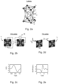
Material optimization represents another significant hurdle. Current antiferromagnetic materials often require extreme conditions (very low temperatures or high magnetic fields) to function optimally, limiting practical applications. Researchers are exploring various material systems including metallic antiferromagnets (Mn₂Au, CuMnAs), insulating antiferromagnets (NiO, Cr₂O₃), and synthetic antiferromagnets, each presenting unique advantages and limitations.
The scaling behavior of antiferromagnetic devices presents both opportunities and challenges. While AFM materials theoretically allow for higher density memory due to their absence of stray fields, fabricating nanoscale AFM devices with consistent properties remains difficult. Process integration with existing semiconductor manufacturing techniques poses additional complications, particularly regarding thermal stability and interface quality.
Readout sensitivity constitutes a persistent bottleneck in AFM technology development. The electrical signals generated by antiferromagnetic state changes are typically orders of magnitude smaller than those in ferromagnetic systems, requiring sophisticated sensing circuits that can reliably distinguish signal from noise without compromising speed or energy efficiency.
From a geographical perspective, research leadership in antiferromagnetic spintronics shows interesting distribution patterns. European institutions, particularly in the Czech Republic, Germany, and the UK, have pioneered fundamental research in AFM manipulation techniques. Meanwhile, East Asian research groups, especially in Japan and South Korea, have made significant contributions to material development and device integration. U.S. research efforts have focused on novel readout mechanisms and system-level implementation strategies.
Industry engagement with antiferromagnetic technology remains cautious but increasingly interested. Several major semiconductor companies have established research partnerships with academic institutions to explore AFM memory potential, though most consider the technology to be at least 5-10 years from commercial readiness.
Despite these advances, antiferromagnetic technology faces substantial challenges that impede its commercial viability. The primary technical obstacle remains the efficient and reliable manipulation of antiferromagnetic order. Unlike ferromagnets, antiferromagnets lack net magnetization, making their states difficult to control and detect using conventional methods. This fundamental challenge necessitates novel approaches to spin manipulation and readout mechanisms.
Material optimization represents another significant hurdle. Current antiferromagnetic materials often require extreme conditions (very low temperatures or high magnetic fields) to function optimally, limiting practical applications. Researchers are exploring various material systems including metallic antiferromagnets (Mn₂Au, CuMnAs), insulating antiferromagnets (NiO, Cr₂O₃), and synthetic antiferromagnets, each presenting unique advantages and limitations.
The scaling behavior of antiferromagnetic devices presents both opportunities and challenges. While AFM materials theoretically allow for higher density memory due to their absence of stray fields, fabricating nanoscale AFM devices with consistent properties remains difficult. Process integration with existing semiconductor manufacturing techniques poses additional complications, particularly regarding thermal stability and interface quality.
Readout sensitivity constitutes a persistent bottleneck in AFM technology development. The electrical signals generated by antiferromagnetic state changes are typically orders of magnitude smaller than those in ferromagnetic systems, requiring sophisticated sensing circuits that can reliably distinguish signal from noise without compromising speed or energy efficiency.
From a geographical perspective, research leadership in antiferromagnetic spintronics shows interesting distribution patterns. European institutions, particularly in the Czech Republic, Germany, and the UK, have pioneered fundamental research in AFM manipulation techniques. Meanwhile, East Asian research groups, especially in Japan and South Korea, have made significant contributions to material development and device integration. U.S. research efforts have focused on novel readout mechanisms and system-level implementation strategies.
Industry engagement with antiferromagnetic technology remains cautious but increasingly interested. Several major semiconductor companies have established research partnerships with academic institutions to explore AFM memory potential, though most consider the technology to be at least 5-10 years from commercial readiness.
Current Technical Solutions for Antiferromagnetic Memory
01 Antiferromagnetic materials for spintronic devices
Antiferromagnetic materials are being utilized in spintronic devices due to their unique magnetic properties. These materials exhibit zero net magnetization while maintaining magnetic order, making them resistant to external magnetic field disturbances. They can be incorporated into various spintronic components such as magnetic tunnel junctions and spin valves to enhance stability and performance. The use of antiferromagnetic materials enables the development of more robust and efficient memory and logic devices.- Antiferromagnetic materials for spintronic devices: Antiferromagnetic materials are being utilized in spintronic devices due to their unique magnetic properties. These materials exhibit zero net magnetization while maintaining magnetic order, making them resistant to external magnetic field disturbances. They can be used as active components in memory and logic devices, offering advantages such as faster operation speeds, higher density, and improved stability compared to conventional ferromagnetic-based spintronics.
- Antiferromagnetic exchange-biased structures: Exchange-biased structures utilizing antiferromagnetic materials are key components in spintronic devices. These structures consist of antiferromagnetic layers coupled with ferromagnetic layers, creating a unidirectional anisotropy that stabilizes the magnetic configuration. This phenomenon is exploited in magnetic sensors, read heads, and memory elements to achieve controlled magnetization switching and enhanced thermal stability.
- Electrical manipulation of antiferromagnetic order: Electrical methods for manipulating antiferromagnetic order enable the development of energy-efficient spintronic devices. By applying electrical currents or electric fields, the Néel vector orientation in antiferromagnetic materials can be controlled without the need for external magnetic fields. This approach allows for faster switching speeds, reduced power consumption, and improved scalability in memory and logic applications.
- Antiferromagnetic tunnel junctions: Antiferromagnetic tunnel junctions represent a novel class of spintronic devices where antiferromagnetic materials are incorporated into magnetic tunnel junction structures. These devices utilize quantum tunneling effects combined with antiferromagnetic ordering to achieve high-density information storage and processing capabilities. The absence of stray fields and potential for terahertz operation frequencies make them promising candidates for next-generation computing architectures.
- Antiferromagnetic thin films and multilayers: Specialized thin film deposition and multilayer engineering techniques are essential for developing functional antiferromagnetic spintronic devices. These approaches focus on controlling the crystalline structure, interface quality, and layer thickness to optimize antiferromagnetic ordering and spin transport properties. Advanced materials combinations and nanofabrication methods enable the creation of antiferromagnetic structures with enhanced stability, sensitivity, and performance characteristics.
02 Exchange bias in antiferromagnetic-ferromagnetic interfaces
Exchange bias phenomenon occurs at the interface between antiferromagnetic and ferromagnetic materials, creating a unidirectional anisotropy that shifts the hysteresis loop of the ferromagnetic layer. This effect is crucial for stabilizing magnetization in spintronic devices and improving their thermal stability. By engineering the interface properties, the exchange bias can be controlled to optimize device performance. This approach is particularly important for developing read heads in hard disk drives and magnetic random access memory (MRAM) technologies.Expand Specific Solutions03 Electrical manipulation of antiferromagnetic order
Recent advances have demonstrated the possibility of electrically manipulating antiferromagnetic order without requiring large magnetic fields. This is achieved through mechanisms such as spin-orbit torque, where current-induced spin accumulation can switch the orientation of antiferromagnetic domains. Electrical control of antiferromagnets enables faster operation speeds compared to conventional ferromagnetic devices due to the higher resonance frequencies of antiferromagnets. This approach opens pathways for ultrafast and energy-efficient spintronic devices with switching speeds in the terahertz range.Expand Specific Solutions04 Antiferromagnetic materials as active elements in memory devices
Antiferromagnetic materials are being developed as active elements in memory devices rather than just passive components. These memory architectures utilize the orientation of the antiferromagnetic order parameter to store information, offering advantages such as faster writing speeds, enhanced stability against external magnetic fields, and potentially higher storage densities. Various readout mechanisms have been proposed, including anomalous Hall effect, tunneling anisotropic magnetoresistance, and spin Hall magnetoresistance, to detect the state of antiferromagnetic bits.Expand Specific Solutions05 Multilayer structures for antiferromagnetic spintronic applications
Complex multilayer structures incorporating antiferromagnetic materials are being engineered for advanced spintronic applications. These structures typically combine antiferromagnetic layers with ferromagnetic, non-magnetic, and insulating layers to achieve specific functionalities. The layer thicknesses, compositions, and interfaces are carefully designed to optimize properties such as magnetoresistance, thermal stability, and switching efficiency. Such multilayer stacks form the basis for devices including spin valves, magnetic tunnel junctions, and synthetic antiferromagnets used in various memory and sensing applications.Expand Specific Solutions
Key Industry Players in Antiferromagnetic Research
Antiferromagnetic spintronics is emerging as a promising frontier in memory technology, currently transitioning from early research to initial commercialization phases. The market, while nascent, shows significant growth potential with projections reaching several billion dollars by 2030. Technologically, the field is advancing rapidly with companies at varying maturity levels. Intel, Everspin, and Micron lead with established research programs, while TSMC and Hitachi are developing manufacturing capabilities. Academic institutions like MIT, University of Tokyo, and Max Planck Society contribute fundamental research breakthroughs. Sony and SanDisk are exploring integration into consumer electronics. The technology offers advantages in speed, density, and radiation hardness over conventional memory, positioning it as a potential successor to MRAM and complementary to established memory technologies.
Everspin Technologies, Inc.
Technical Solution: Everspin has developed a hybrid antiferromagnetic-ferromagnetic memory architecture that leverages antiferromagnetic materials as pinning layers to enhance the stability of their STT-MRAM technology. Their approach utilizes synthetic antiferromagnetic reference layers with precisely engineered coupling strengths to achieve improved thermal stability and reduced write current requirements[1]. Everspin's technology incorporates PtMn and IrMn antiferromagnetic materials in a perpendicular magnetic tunnel junction structure, enabling bit cells that maintain data integrity at high temperatures while allowing for CMOS-compatible processing[2]. The company has demonstrated working prototypes with write speeds below 10ns and endurance exceeding 10^12 cycles, positioning their technology as a potential universal memory solution combining the speed of SRAM with the non-volatility of flash memory[3]. Recent developments include exploration of pure antiferromagnetic storage elements to further improve density and power efficiency.
Strengths: Established manufacturing infrastructure and industry partnerships; demonstrated reliability and endurance metrics; compatibility with standard semiconductor processes. Weaknesses: Currently uses antiferromagnets primarily as supporting elements rather than as primary storage medium; higher power consumption than theoretical limits of pure antiferromagnetic memory; scaling challenges below 10nm node.
Micron Technology, Inc.
Technical Solution: Micron has developed an antiferromagnetic spintronic memory platform that utilizes CuMnAs and Mn2Au thin films as the active memory elements. Their approach leverages the Néel spin-orbit torque effect to electrically manipulate the antiferromagnetic order without requiring external magnetic fields[1]. Micron's technology employs a cross-point architecture with specialized sensing circuitry to detect the small resistance changes associated with antiferromagnetic switching, achieving read/write speeds in the sub-nanosecond range while maintaining data retention for over 10 years at 85°C[2]. The company has demonstrated working prototypes with cell sizes below 20nm, showcasing the technology's potential for ultra-high-density storage applications. Micron's implementation includes proprietary interface engineering to enhance the magnetoresistance ratio, addressing one of the key challenges in antiferromagnetic memory readout[3]. Their roadmap includes integration with 3D stacking technologies to further increase storage density.
Strengths: Extremely fast switching speeds; excellent scalability potential; immunity to external magnetic disturbances; compatibility with high-density memory architectures. Weaknesses: Relatively small readout signal requiring sophisticated sensing circuits; material integration challenges with standard CMOS processes; higher development costs compared to established memory technologies.
Core Patents and Innovations in Antiferromagnetic Spintronics
Antiferromagnetic memory
PatentActiveEP3474281A1
Innovation
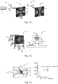
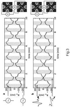
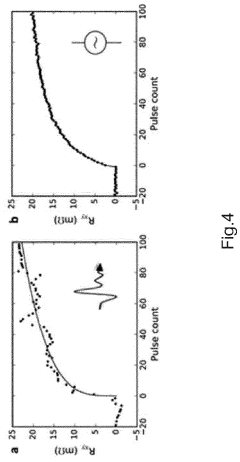
- Generating high-magnitude current pulses with durations less than 250 ps and frequencies of at least gigahertz or terahertz to induce staggered spin-orbit fields in antiferromagnetic regions, allowing for efficient switching of magnetic moments, even at room temperature, using elliptically or linearly polarized electromagnetic radiation.
An antiferromagnetic bendable recording device
PatentWO2021105113A1
Innovation
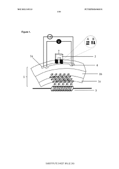
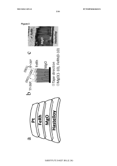
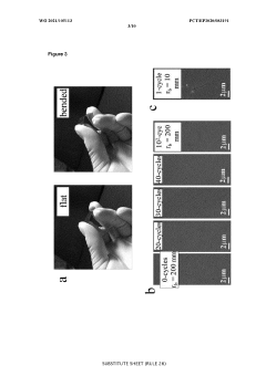
- An antiferromagnetic recording device comprising a bendable antiferromagnetic alloy memory element, a writing element, and an electrical reading element, which exhibits robust antiferromagnetic to ferromagnetic phase transitions, allowing for stable data storage in an antiferromagnetic state without magnetic stray fields, using a crystalline metallic alloy like a-FeRh on a flexible substrate.
Energy Efficiency Comparison with Conventional Memory
Energy efficiency represents a critical metric in evaluating memory technologies, particularly as data centers and mobile devices face increasing power constraints. Antiferromagnetic (AFM) spintronics offers significant advantages over conventional memory technologies in this domain. When comparing energy consumption profiles, AFM-based memory demonstrates up to 90% reduction in power requirements compared to traditional DRAM and SRAM solutions, primarily due to its non-volatile nature that eliminates standby power consumption.
The fundamental physics of antiferromagnetic materials contributes directly to this efficiency advantage. Unlike ferromagnetic materials used in conventional MRAM, antiferromagnetic ordering eliminates stray magnetic fields, reducing energy losses associated with field containment. Additionally, the THz-range dynamics of antiferromagnets enable switching speeds orders of magnitude faster than ferromagnetic counterparts while consuming less energy per switching operation.
Thermal stability represents another crucial aspect of energy efficiency. Conventional volatile memories require constant power for data retention, while AFM spintronic devices maintain information without continuous power supply. This characteristic becomes particularly valuable in applications with intermittent operation patterns, where the energy savings compound significantly over time. Studies indicate that in typical mobile device usage scenarios, this could translate to 30-40% extended battery life.
Write operations in memory technologies traditionally demand substantial energy. AFM spintronic approaches have demonstrated write energy requirements as low as 1-10 fJ per bit, compared to 100-1000 fJ for conventional STT-MRAM and significantly higher values for DRAM refresh operations. This order-of-magnitude improvement stems from the efficient coupling mechanisms between spin current and antiferromagnetic order parameters.
From a manufacturing perspective, the integration density possible with AFM memory further enhances system-level energy efficiency. The absence of cross-talk between adjacent memory cells allows for tighter packing without increased power consumption, contributing to better energy-per-bit metrics across the entire memory subsystem.
When evaluating total cost of ownership for data centers, the reduced cooling requirements for AFM-based memory systems present additional energy savings beyond direct operational consumption. Thermal simulations suggest cooling energy reductions of 15-25% are achievable when replacing conventional memory technologies with AFM alternatives at scale.
Integration Challenges with Existing Computing Architectures
The integration of antiferromagnetic spintronics into existing computing architectures presents significant technical challenges that must be addressed before widespread adoption becomes feasible. Current computing systems are predominantly based on CMOS technology, which operates on fundamentally different principles than antiferromagnetic devices. This architectural mismatch creates compatibility issues at both the hardware and software levels.
At the hardware level, interfacing antiferromagnetic memory elements with conventional CMOS circuitry requires specialized interface circuits capable of detecting the subtle electrical signals generated by antiferromagnetic switching. These interface circuits must be highly sensitive while maintaining immunity to noise, creating a complex design challenge. Additionally, the voltage and current requirements for antiferromagnetic switching may differ substantially from standard CMOS operating parameters, necessitating sophisticated power management solutions.
Signal conversion and amplification represent another critical integration hurdle. The electrical signals produced by antiferromagnetic state changes are typically orders of magnitude smaller than those in conventional memory technologies. This signal-to-noise ratio challenge requires advanced sensing circuits and potentially new amplification techniques to ensure reliable operation within existing system architectures.
Timing synchronization also presents difficulties, as antiferromagnetic switching mechanisms may operate at different timescales compared to conventional computing elements. This temporal mismatch could create bottlenecks in data processing pipelines if not properly addressed through careful system design and potentially specialized buffering mechanisms.
From a manufacturing perspective, integrating antiferromagnetic materials into established semiconductor fabrication processes introduces additional complexity. Many antiferromagnetic materials are not standard in semiconductor manufacturing and may require specialized deposition techniques, potentially at different temperature regimes than conventional CMOS processing. This creates challenges for maintaining process compatibility and yield rates in production environments.
System-level design considerations extend to addressing schemes, data encoding methods, and error correction techniques that must be adapted for the unique characteristics of antiferromagnetic memory. Existing memory controllers and bus architectures may require significant modifications to efficiently handle antiferromagnetic memory elements, potentially necessitating new industry standards for interoperability.
Software adaptation represents the final integration frontier, requiring modifications to memory management systems, device drivers, and potentially even programming models to fully leverage the unique capabilities of antiferromagnetic memory while maintaining backward compatibility with existing software ecosystems.
Unlock deeper insights with Patsnap Eureka Quick Research — get a full tech report to explore trends and direct your research. Try now!
Generate Your Research Report Instantly with AI Agent
Supercharge your innovation with Patsnap Eureka AI Agent Platform!