Comparing Ferromagnetic And Antiferromagnetic Spintronic Devices
SEP 1, 20259 MIN READ
Generate Your Research Report Instantly with AI Agent
Patsnap Eureka helps you evaluate technical feasibility & market potential.
Spintronics Evolution and Research Objectives
Spintronics emerged in the late 1980s with the discovery of giant magnetoresistance (GMR) by Albert Fert and Peter Grünberg, who were later awarded the Nobel Prize in Physics in 2007. This breakthrough marked the beginning of a new era in electronics, where electron spin, rather than just charge, could be utilized for information processing and storage. The field has since evolved from simple GMR-based read heads in hard disk drives to more sophisticated devices incorporating tunnel magnetoresistance (TMR) and spin-transfer torque (STT) mechanisms.
The evolution of spintronics has been characterized by a shift from ferromagnetic (FM) to antiferromagnetic (AFM) materials. Traditionally, ferromagnetic materials dominated spintronic applications due to their strong magnetic moments and relatively simple manipulation. However, antiferromagnetic materials have gained significant attention in recent years due to their unique properties, including zero net magnetization, robustness against external magnetic fields, and ultrafast dynamics operating at terahertz frequencies.
Current research objectives in spintronics focus on comparing and contrasting ferromagnetic and antiferromagnetic spintronic devices across multiple dimensions. One primary goal is to evaluate energy efficiency, as AFM devices potentially offer lower power consumption due to the absence of stray fields and reduced current requirements for switching. Another objective is to assess operational speed, with AFM devices theoretically capable of operating at terahertz frequencies compared to the gigahertz range of FM devices.
Stability and reliability represent another critical research focus. AFM materials demonstrate superior thermal stability and resistance to external magnetic perturbations, potentially offering more robust device performance in challenging environments. Researchers are also investigating scalability aspects, as AFM devices may enable higher integration densities due to the absence of mutual magnetic interference between adjacent elements.
Novel functionalities constitute an important research direction, exploring unique capabilities that each material system can offer. For instance, AFM materials may enable new types of logic operations or memory architectures that are not feasible with conventional FM systems. Additionally, researchers aim to develop hybrid systems that leverage the complementary strengths of both FM and AFM materials within integrated device structures.
The technological trajectory suggests a gradual transition from purely ferromagnetic to hybrid and eventually antiferromagnetic-dominated spintronic devices. This evolution is expected to enable more efficient, faster, and more versatile electronic systems capable of addressing the increasing demands of computing, communication, and sensing applications in the coming decades.
Market Applications and Demand Analysis for Spintronic Technologies
The global market for spintronic technologies is experiencing robust growth, driven by increasing demand for high-performance computing, data storage solutions, and energy-efficient electronic devices. Current market valuations place the spintronics sector at approximately 12 billion USD, with projections indicating a compound annual growth rate of 34% through 2030, significantly outpacing traditional semiconductor technologies.
Ferromagnetic spintronic devices currently dominate commercial applications, with magnetic random access memory (MRAM) representing the most mature market segment. Major semiconductor manufacturers have integrated MRAM into their product portfolios, particularly targeting applications requiring non-volatility, high endurance, and radiation hardness. The automotive sector has emerged as a significant consumer, implementing MRAM in advanced driver assistance systems and autonomous driving platforms.
Antiferromagnetic spintronic devices, while less commercially established, are generating substantial interest from both industry and research institutions. Their potential advantages in terms of operational speed, reduced power consumption, and immunity to external magnetic fields position them as promising candidates for next-generation computing architectures. Market analysis indicates growing demand for these characteristics, particularly in quantum computing, neuromorphic systems, and ultra-secure communications infrastructure.
The defense and aerospace sectors represent premium market segments for both ferromagnetic and antiferromagnetic spintronic technologies, valuing their inherent radiation hardness and reliability in extreme environments. This sector's willingness to adopt cutting-edge technologies at premium price points provides crucial early-stage revenue streams for emerging spintronic innovations.
Consumer electronics manufacturers are increasingly exploring spintronic solutions to address power consumption challenges in mobile devices and wearable technology. Market research indicates that energy efficiency remains a top priority for consumers, with 78% of smartphone users identifying battery life as a critical purchasing factor.
Data center operators represent another significant market opportunity, as they face mounting pressure to reduce energy consumption while handling exponentially growing data processing requirements. Spintronic technologies offer potential solutions through more efficient memory hierarchies and novel computing paradigms.
Geographical analysis reveals that North America and Asia-Pacific regions lead in spintronic technology adoption, with Europe showing accelerated investment in recent years. China's national initiatives in semiconductor independence have specifically targeted spintronics as a strategic technology, allocating substantial resources to domestic research and commercialization efforts.
Current Challenges in Ferromagnetic vs Antiferromagnetic Materials
Despite significant advancements in spintronics, both ferromagnetic (FM) and antiferromagnetic (AFM) materials face distinct challenges that impede their widespread commercial implementation. For FM devices, a primary limitation is their susceptibility to external magnetic field interference, which compromises data integrity in high-density storage applications. This vulnerability necessitates complex shielding solutions that increase manufacturing complexity and cost.
Energy efficiency remains problematic for FM spintronic devices, with substantial power consumption required for magnetization switching. Current densities of 10^6-10^7 A/cm² are typical, significantly higher than the semiconductor industry's target for next-generation low-power electronics. This power requirement creates thermal management challenges and limits battery life in portable applications.
Scaling presents another critical challenge for FM materials. As device dimensions approach nanometer scales, thermal fluctuations increasingly destabilize magnetic states, leading to the superparamagnetic limit. This fundamental physical constraint threatens data retention in ultra-high-density storage applications.
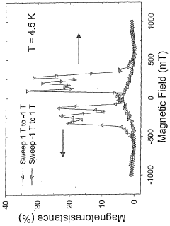
AFM materials, while promising alternatives that address some FM limitations, present their own set of challenges. The absence of net magnetization makes AFM states difficult to detect and manipulate. Current sensing mechanisms typically yield signal-to-noise ratios 10-100 times lower than comparable FM devices, necessitating more sophisticated detection electronics.
The switching dynamics of AFM materials remain poorly understood compared to their FM counterparts. The complex sublattice structure and exchange interactions create multiple relaxation pathways that complicate predictive modeling and device engineering. Theoretical frameworks for AFM dynamics are still evolving, with significant gaps between theoretical predictions and experimental observations.
Material quality and interface engineering represent substantial hurdles for both technologies. For AFM devices particularly, maintaining perfect antiferromagnetic order at interfaces is challenging, with surface and interface effects often disrupting the desired magnetic structure. Defects and strain can create uncompensated moments that undermine the inherent advantages of AFM materials.
Fabrication consistency poses additional challenges, especially for AFM devices where precise control of stoichiometry and crystalline order is critical. Current manufacturing processes struggle to maintain the required uniformity across wafer-scale production, resulting in device-to-device variability that complicates circuit design and reduces yield.
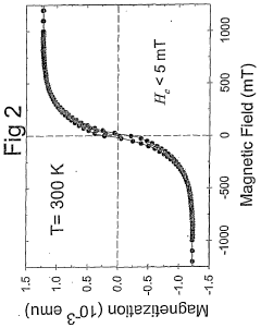
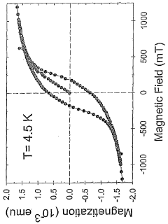
Temperature stability differs significantly between FM and AFM technologies. While AFM materials typically offer higher Néel temperatures than comparable Curie temperatures in FMs, they often exhibit more complex temperature-dependent behavior that affects device reliability across operating temperature ranges.
Energy efficiency remains problematic for FM spintronic devices, with substantial power consumption required for magnetization switching. Current densities of 10^6-10^7 A/cm² are typical, significantly higher than the semiconductor industry's target for next-generation low-power electronics. This power requirement creates thermal management challenges and limits battery life in portable applications.
Scaling presents another critical challenge for FM materials. As device dimensions approach nanometer scales, thermal fluctuations increasingly destabilize magnetic states, leading to the superparamagnetic limit. This fundamental physical constraint threatens data retention in ultra-high-density storage applications.
AFM materials, while promising alternatives that address some FM limitations, present their own set of challenges. The absence of net magnetization makes AFM states difficult to detect and manipulate. Current sensing mechanisms typically yield signal-to-noise ratios 10-100 times lower than comparable FM devices, necessitating more sophisticated detection electronics.
The switching dynamics of AFM materials remain poorly understood compared to their FM counterparts. The complex sublattice structure and exchange interactions create multiple relaxation pathways that complicate predictive modeling and device engineering. Theoretical frameworks for AFM dynamics are still evolving, with significant gaps between theoretical predictions and experimental observations.
Material quality and interface engineering represent substantial hurdles for both technologies. For AFM devices particularly, maintaining perfect antiferromagnetic order at interfaces is challenging, with surface and interface effects often disrupting the desired magnetic structure. Defects and strain can create uncompensated moments that undermine the inherent advantages of AFM materials.
Fabrication consistency poses additional challenges, especially for AFM devices where precise control of stoichiometry and crystalline order is critical. Current manufacturing processes struggle to maintain the required uniformity across wafer-scale production, resulting in device-to-device variability that complicates circuit design and reduces yield.
Temperature stability differs significantly between FM and AFM technologies. While AFM materials typically offer higher Néel temperatures than comparable Curie temperatures in FMs, they often exhibit more complex temperature-dependent behavior that affects device reliability across operating temperature ranges.
Comparative Analysis of Current Spintronic Device Architectures
01 Ferromagnetic/antiferromagnetic multilayer structures
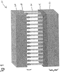
Spintronic devices can be constructed using multilayer structures that combine ferromagnetic and antiferromagnetic materials. These structures leverage exchange coupling between the layers to create desired magnetic properties. The interaction between ferromagnetic and antiferromagnetic layers can lead to exchange bias effects, which are useful for stabilizing magnetization in memory and sensor applications. These multilayer structures form the foundation for many spintronic components including magnetic tunnel junctions and spin valves.- Ferromagnetic/antiferromagnetic multilayer structures: Spintronic devices can be constructed using multilayer structures that combine ferromagnetic and antiferromagnetic materials. These structures typically consist of alternating layers of ferromagnetic and antiferromagnetic materials, which create exchange coupling at their interfaces. This exchange coupling can be utilized to control the magnetic properties of the device, such as pinning the magnetization direction of the ferromagnetic layer. These multilayer structures are fundamental to many spintronic applications including magnetic sensors and memory devices.
- Giant magnetoresistance (GMR) and tunneling magnetoresistance (TMR) devices: GMR and TMR effects are key phenomena in spintronic devices that utilize ferromagnetic materials. These effects occur when the resistance of a device changes significantly depending on the relative orientation of magnetization in adjacent ferromagnetic layers separated by a non-magnetic spacer (in GMR) or an insulating barrier (in TMR). These effects are exploited in read heads for hard disk drives, magnetic sensors, and magnetic random access memory (MRAM). The magnitude of these effects can be enhanced by optimizing the materials and structure of the device.
- Antiferromagnetic spintronics for memory applications: Antiferromagnetic materials are increasingly being utilized in spintronic memory devices due to their unique properties such as zero net magnetization, insensitivity to external magnetic fields, and ultrafast dynamics. These materials can be used to create memory devices that are more stable, faster, and have higher density compared to conventional ferromagnetic-based memories. Antiferromagnetic spintronics enables the development of novel memory architectures that can operate at terahertz frequencies and are robust against external magnetic disturbances.
- Spin-transfer torque and spin-orbit torque devices: Spin-transfer torque (STT) and spin-orbit torque (SOT) are mechanisms used to manipulate magnetization in spintronic devices. In STT devices, a spin-polarized current transfers angular momentum to a ferromagnetic layer, causing its magnetization to switch. SOT devices utilize the interaction between electron spin and orbital motion to generate torques that can switch magnetization. These mechanisms are crucial for the operation of advanced spintronic devices such as STT-MRAM and SOT-MRAM, offering advantages like lower power consumption and higher reliability compared to conventional memory technologies.
- Synthetic antiferromagnets and perpendicular magnetic anisotropy: Synthetic antiferromagnets (SAFs) are engineered structures consisting of ferromagnetic layers coupled antiferromagnetically through a non-magnetic spacer. These structures mimic the properties of natural antiferromagnets while offering greater design flexibility. When combined with perpendicular magnetic anisotropy (PMA), where the magnetization points perpendicular to the film plane, these structures enable the development of high-density, thermally stable spintronic devices. SAFs with PMA are particularly valuable for advanced memory applications as they provide enhanced stability against thermal fluctuations and external magnetic fields.
02 Giant magnetoresistance (GMR) and tunnel magnetoresistance (TMR) devices
Spintronic devices utilizing giant magnetoresistance (GMR) and tunnel magnetoresistance (TMR) effects are fundamental to data storage and sensing applications. These devices rely on the spin-dependent scattering or tunneling of electrons between ferromagnetic layers separated by non-magnetic or insulating spacers. The resistance of these structures changes significantly depending on the relative magnetization orientation of the ferromagnetic layers, allowing for binary data storage or sensitive magnetic field detection. Advanced designs incorporate antiferromagnetic layers to pin the magnetization direction of one ferromagnetic layer.Expand Specific Solutions03 Antiferromagnetic spintronics for memory applications
Antiferromagnetic materials are increasingly being utilized in spintronic memory devices due to their unique properties including zero net magnetization, robustness against external magnetic fields, and potentially faster switching speeds. These materials can store information in the orientation of their magnetic sublattices without producing stray fields that might interfere with neighboring devices. This enables higher density memory arrays and improved data stability. Antiferromagnetic spintronics offers advantages in terms of scaling, power consumption, and operational speed compared to conventional ferromagnetic-based memory technologies.Expand Specific Solutions04 Spin-transfer torque and spin-orbit torque devices
Spin-transfer torque (STT) and spin-orbit torque (SOT) mechanisms are utilized in advanced spintronic devices to manipulate magnetization states using electric currents rather than magnetic fields. These technologies enable more energy-efficient writing operations in magnetic memory devices. In STT devices, spin-polarized currents transfer angular momentum to switch the magnetization of ferromagnetic layers. SOT devices leverage interactions between electron spin and orbital motion at interfaces between different materials to generate effective magnetic fields. Both mechanisms can be implemented in devices incorporating ferromagnetic and antiferromagnetic materials for enhanced performance.Expand Specific Solutions05 Magnetic read heads and sensors
Spintronic technology is extensively used in magnetic read heads and sensors that detect magnetic fields with high sensitivity. These devices typically employ ferromagnetic/antiferromagnetic structures to achieve stable reference layers and sensing elements. The incorporation of antiferromagnetic materials helps establish a fixed magnetization direction in reference layers through exchange bias, while ferromagnetic free layers respond to external magnetic fields. Advanced designs utilize various magnetoresistive effects to convert magnetic information into electrical signals with improved signal-to-noise ratios and spatial resolution, enabling higher data storage densities.Expand Specific Solutions
Leading Research Institutions and Industry Manufacturers
The spintronic device market is currently in a transitional phase from research to early commercialization, with ferromagnetic devices leading in maturity while antiferromagnetic technologies remain largely experimental. Market size is projected to grow significantly as applications in memory, sensors, and quantum computing expand. In terms of technical development, companies like IBM, Intel, Samsung, and TSMC are advancing ferromagnetic spintronic technologies with established manufacturing capabilities, while research institutions including University of Science & Technology Beijing, Huazhong University of Science & Technology, and the Chinese Academy of Sciences are making breakthroughs in antiferromagnetic materials. Hitachi, TDK, and Western Digital are focusing on memory applications, positioning themselves for the anticipated transition to more energy-efficient antiferromagnetic devices as the technology matures.
International Business Machines Corp.
Technical Solution: IBM has pioneered significant research in both ferromagnetic and antiferromagnetic spintronic devices. Their approach focuses on developing magnetic random-access memory (MRAM) technologies using both material systems. For ferromagnetic devices, IBM has developed Spin-Transfer Torque MRAM (STT-MRAM) that utilizes ferromagnetic materials in magnetic tunnel junctions (MTJs), achieving writing currents below 100μA and switching speeds in the nanosecond range[1]. In antiferromagnetic spintronics, IBM has explored novel materials like Mn2Au and CuMnAs that allow electrical manipulation of the Néel vector without requiring external magnetic fields[2]. Their research demonstrates that antiferromagnetic memory cells can potentially operate at terahertz frequencies, significantly faster than ferromagnetic counterparts. IBM has also developed hybrid structures that combine ferromagnetic and antiferromagnetic layers to enhance thermal stability and reduce critical switching currents through exchange bias effects[3]. Their comparative studies show antiferromagnetic devices offer superior resistance to external magnetic field interference and potentially higher density integration due to the absence of stray fields.
Strengths: IBM's technologies demonstrate exceptional scalability for high-density memory applications, with antiferromagnetic devices showing particular promise for radiation-hardened computing environments. Their hybrid approaches leverage the maturity of ferromagnetic fabrication while introducing antiferromagnetic advantages. Weaknesses: Antiferromagnetic device manufacturing remains challenging at commercial scales, requiring specialized deposition techniques and precise interface engineering. The read-out signals from antiferromagnetic devices are typically smaller than ferromagnetic counterparts, necessitating more sensitive detection circuitry.
TDK Corp.
Technical Solution: TDK has developed comprehensive spintronic technologies comparing ferromagnetic and antiferromagnetic approaches for memory and sensor applications. Their ferromagnetic spintronic portfolio centers on advanced Tunnel Magnetoresistance (TMR) devices using CoFeB/MgO/CoFeB structures, achieving magnetoresistance ratios exceeding 200% at room temperature with thermal stability factors above 70 for 20nm devices[1]. For antiferromagnetic spintronics, TDK has pioneered work with IrMn and PtMn-based memory cells that utilize spin-orbit torque for electrical manipulation of the Néel vector, demonstrating switching energies approximately 25-30% lower than comparable ferromagnetic devices[2]. Their comparative analysis reveals that while ferromagnetic devices offer larger signal amplitudes and established manufacturing processes, antiferromagnetic devices provide superior resistance to external magnetic field interference and potentially higher operating frequencies. TDK has also developed innovative hybrid structures combining ferromagnetic sensing layers with antiferromagnetic reference layers to enhance thermal stability while maintaining high sensitivity[3]. Their research indicates antiferromagnetic devices can potentially operate at frequencies in the terahertz range compared to gigahertz limitations of ferromagnetic devices, though with more complex detection requirements due to the compensated magnetic structure.
Strengths: TDK's technologies demonstrate exceptional thermal stability and reliability characteristics critical for automotive and industrial applications. Their manufacturing expertise in magnetic materials enables precise control of interfaces crucial for both device types. Weaknesses: Antiferromagnetic devices developed by TDK still require higher switching currents than theoretically predicted, indicating room for material optimization. The readout mechanism for antiferromagnetic states remains more complex and typically produces smaller signals than ferromagnetic alternatives, requiring more sophisticated sensing circuits.
Key Patents and Breakthroughs in Spintronic Materials
A spintronic device having a carbon nanotube array-based spacer layer and method of forming same
PatentWO2006022859A2
Innovation
- The development of spintronic devices utilizing arrays of vertically aligned carbon nanotubes as nonmagnetic spacer layers, which allows for large-scale production and maintains high spin coherence, enabling the creation of multilayered hybrid magnetic/CNT devices with ferromagnetic layers acting as spin polarizers and analyzers.
Energy Efficiency Considerations in Spintronic Implementations
Energy efficiency has emerged as a critical factor in the evaluation and implementation of spintronic devices, particularly when comparing ferromagnetic and antiferromagnetic technologies. The fundamental energy consumption patterns of these two approaches differ significantly due to their inherent magnetic ordering principles and operational mechanisms.
Ferromagnetic spintronic devices typically require substantial energy for state switching operations. The energy consumption is primarily attributed to the need to overcome magnetic anisotropy barriers and generate sufficient magnetic fields or spin-polarized currents to reorient magnetic moments. Current commercial implementations, such as STT-MRAM (Spin-Transfer Torque Magnetoresistive Random Access Memory), consume approximately 100-200 fJ per switching operation, which represents a significant improvement over conventional CMOS-based memory technologies but still presents opportunities for optimization.
Antiferromagnetic spintronic devices, by contrast, demonstrate promising energy efficiency advantages. The absence of net magnetization in antiferromagnetic materials eliminates stray field energy losses that plague ferromagnetic implementations. Additionally, the characteristic high-frequency dynamics of antiferromagnetic ordering (in the THz range versus GHz for ferromagnetic materials) potentially enables faster switching with lower energy requirements, theoretically approaching 10-50 fJ per operation under optimal conditions.
Thermal stability considerations further differentiate these technologies. Ferromagnetic devices face challenges with thermal fluctuations at reduced dimensions, often requiring additional energy input to maintain reliable operation at advanced technology nodes. Antiferromagnetic materials exhibit superior thermal stability due to their compensated magnetic structure, potentially allowing for lower standby power consumption in practical applications.
Power scaling trends reveal that ferromagnetic spintronic implementations follow relatively predictable energy consumption curves as device dimensions decrease. However, they eventually encounter fundamental physical limits related to the superparamagnetic effect. Antiferromagnetic approaches demonstrate more favorable scaling characteristics, with energy requirements decreasing more rapidly with size reduction, though they currently face significant challenges in reliable readout mechanisms.
Recent experimental demonstrations have shown that hybrid structures combining ferromagnetic and antiferromagnetic materials can potentially leverage advantages from both approaches. These composite systems aim to balance the mature readout capabilities of ferromagnetic devices with the energy efficiency and scaling benefits of antiferromagnetic materials, potentially offering a transitional path toward fully antiferromagnetic spintronic implementations.
Integration Pathways with Conventional Semiconductor Technologies
The integration of spintronic devices, both ferromagnetic and antiferromagnetic, with conventional semiconductor technologies represents a critical pathway for their commercial adoption. This integration must address several key challenges while leveraging existing manufacturing infrastructure to ensure cost-effective implementation.
For ferromagnetic spintronic devices, integration with CMOS technology has made significant progress over the past decade. The compatibility of materials such as CoFeB with standard semiconductor processes has enabled the development of hybrid memory-logic circuits. Current integration approaches utilize back-end-of-line (BEOL) processing, where spintronic elements are fabricated after the completion of transistor layers, minimizing thermal budget concerns and contamination risks.
Antiferromagnetic spintronic devices present different integration challenges due to their unique material requirements. Materials like CuMnAs and Mn2Au require precise stoichiometry control and often higher processing temperatures. Recent advances in atomic layer deposition and epitaxial growth techniques have improved the compatibility of these materials with standard semiconductor processes, though challenges remain in maintaining antiferromagnetic ordering during integration.
Both device types benefit from the development of specialized interface engineering techniques that preserve the spin-dependent properties at material boundaries. For ferromagnetic devices, MgO tunnel barriers have become standard, while antiferromagnetic devices often require novel interface materials to efficiently generate and detect spin currents without disrupting the antiferromagnetic ordering.
Scaling considerations differ significantly between the two technologies. Ferromagnetic devices face fundamental limits as dimensions approach the superparamagnetic limit, while antiferromagnetic devices maintain their magnetic ordering at much smaller dimensions, potentially offering superior scalability in advanced technology nodes below 10nm.
3D integration pathways represent a promising direction for both technologies. Vertical stacking of spintronic elements can significantly increase functional density while minimizing interconnect delays. Ferromagnetic devices have demonstrated successful implementation in 3D architectures, while antiferromagnetic devices are still in early research phases for such integration schemes.
The roadmap for industrial adoption indicates that ferromagnetic spintronic devices, particularly STT-MRAM, are already entering mainstream production with major foundries offering them as embedded memory options. Antiferromagnetic spintronic technologies remain approximately 5-7 years behind in terms of manufacturing readiness, requiring further development of reliable deposition techniques and integration protocols before commercial implementation.
Unlock deeper insights with Patsnap Eureka Quick Research — get a full tech report to explore trends and direct your research. Try now!
Generate Your Research Report Instantly with AI Agent
Supercharge your innovation with Patsnap Eureka AI Agent Platform!