Scalability: Crossbar And 3D Integration Prospects For AFM Memory
SEP 1, 202510 MIN READ
Generate Your Research Report Instantly with AI Agent
Patsnap Eureka helps you evaluate technical feasibility & market potential.
AFM Memory Evolution and Integration Objectives
Antiferromagnetic (AFM) memory technology has evolved significantly over the past decade, transitioning from theoretical concepts to experimental prototypes with promising characteristics. The evolution began with the discovery of electrical manipulation of antiferromagnetic order in 2014, which opened new possibilities for spintronic devices beyond traditional ferromagnetic materials. This breakthrough demonstrated that AFM materials could serve as active components in memory devices rather than merely passive elements.
The development trajectory has been marked by several key milestones, including the demonstration of electrical reading of AFM states, room-temperature operation, and nanosecond switching capabilities. Early AFM memory concepts faced significant challenges in reliable reading and writing operations, but recent advancements in spin-orbit torque mechanisms and detection techniques have substantially improved device performance and reliability.
Current integration objectives for AFM memory focus on achieving competitive metrics compared to established memory technologies while leveraging the unique advantages of antiferromagnetism. Primary goals include reducing switching energy below 1 pJ, decreasing switching times to sub-nanosecond range, and ensuring retention times exceeding 10 years for non-volatile applications. Additionally, integration efforts aim to achieve bit densities comparable to or exceeding DRAM while maintaining CMOS compatibility.
Scalability represents a central objective in AFM memory development, with crossbar architectures emerging as a promising approach. The crossbar configuration allows for high-density memory arrays with minimal cell area, theoretically approaching 4F² in planar implementations. This architecture also facilitates straightforward addressing schemes and reduces line resistance issues that plague other memory technologies at advanced nodes.
3D integration presents perhaps the most ambitious objective for AFM memory technology, with the potential to dramatically increase storage density through vertical stacking. Unlike conventional magnetic memories that suffer from interlayer interference, AFM materials' absence of stray fields makes them particularly suitable for 3D integration. Current research focuses on developing fabrication processes that enable multiple layers of AFM memory cells while maintaining thermal budgets compatible with back-end-of-line processing.
Integration objectives also encompass reliability and endurance improvements, targeting cycling capabilities exceeding 10¹⁵ cycles to compete with emerging non-volatile memories. Temperature stability across a wide operating range (-40°C to 125°C) represents another critical goal for automotive and industrial applications. These objectives collectively aim to position AFM memory as a viable technology for next-generation computing systems, potentially bridging the performance gap between volatile and non-volatile memory technologies.
Market Analysis for High-Density Non-Volatile Memory
The non-volatile memory (NVM) market is experiencing significant growth, driven by increasing demand for high-density storage solutions across various sectors including consumer electronics, automotive, enterprise storage, and emerging IoT applications. Current market projections indicate that the global NVM market will reach approximately $120 billion by 2026, with a compound annual growth rate exceeding 10% from 2021 to 2026.
High-density memory solutions, particularly those leveraging advanced technologies like AFM (Atomic Force Microscopy) memory with crossbar architecture and 3D integration capabilities, are positioned to capture substantial market share. This growth is primarily fueled by the exponential increase in data generation and the need for faster, more energy-efficient storage solutions with greater capacity.
The demand for AFM memory is particularly strong in data centers and cloud computing environments, where storage density and power efficiency are critical factors. Market research indicates that data center operators are willing to pay premium prices for memory solutions that can reduce their total cost of ownership through improved density and lower power consumption, which AFM memory with crossbar architecture promises to deliver.
Consumer electronics represents another significant market segment, with smartphone manufacturers seeking higher capacity storage solutions that consume less power. The miniaturization trend in consumer devices creates a natural market pull for the dimensional advantages offered by 3D integration in AFM memory technologies.
Automotive and industrial applications are emerging as high-growth segments for advanced NVM solutions. The increasing complexity of automotive systems, particularly with the rise of autonomous vehicles, requires robust, high-density memory capable of operating in harsh environments. AFM memory's potential for radiation hardness and temperature stability makes it particularly attractive for these applications.
Geographically, North America and Asia-Pacific dominate the market for advanced memory technologies. North America leads in research and development, while Asia-Pacific, particularly Taiwan, South Korea, and China, leads in manufacturing capacity and adoption rates. Europe shows growing interest, particularly in automotive and industrial applications.
Market barriers for AFM memory adoption include high initial manufacturing costs, technical challenges in scaling production, and competition from established technologies like NAND and emerging alternatives such as MRAM and ReRAM. However, the potential density improvements offered by crossbar architecture and 3D integration could provide AFM memory with a significant competitive advantage if manufacturing challenges can be overcome.
Customer willingness to adopt new memory technologies is heavily influenced by compatibility with existing systems, reliability metrics, and total cost considerations. Market research suggests that a 30-40% improvement in density or power efficiency would be required to drive widespread adoption of AFM memory solutions over current technologies.
Crossbar Architecture Challenges and Limitations
Crossbar architectures represent a promising approach for AFM (Atomic Force Microscopy) memory implementation due to their high density and relatively simple structure. However, several significant challenges and limitations impede their widespread adoption and scalability. The fundamental issue lies in the sneak path problem, where unintended current paths through neighboring memory cells during read operations cause interference and misreads. This phenomenon becomes increasingly problematic as array sizes scale up, leading to exponential growth in leakage currents and signal degradation.
The selector device integration presents another major hurdle. While selectors are essential to mitigate sneak paths, incorporating them into each crosspoint introduces additional complexity. Current selector technologies often struggle to meet the combined requirements of high on/off ratios, fast switching speeds, and compatibility with AFM memory materials. The trade-off between selector performance and fabrication complexity directly impacts manufacturing yield and cost-effectiveness.
Line resistance effects become increasingly pronounced in larger crossbar arrays. As row and line lengths extend, the accumulated resistance creates voltage drops that result in non-uniform programming conditions across the array. Cells furthest from drivers receive significantly lower effective voltages than those near drivers, causing inconsistent write operations and reliability issues. This phenomenon establishes practical limits on maximum array dimensions without implementing complex compensation schemes.
Parasitic capacitance between crossing lines introduces additional challenges, particularly affecting switching speed and energy consumption. As crossbar dimensions increase, the cumulative effect of these parasitic elements leads to increased RC delays and signal distortion, ultimately constraining operational frequency and response time of the memory system.
Manufacturing precision requirements pose significant scaling barriers. Crossbar architectures demand extremely precise alignment between perpendicular conductive lines, with tolerance requirements becoming more stringent as feature sizes decrease. Current lithography techniques struggle to maintain the necessary precision at ultra-small dimensions, leading to increased defect rates and yield challenges in high-density implementations.
Heat dissipation represents another critical limitation. The dense packing of memory cells in crossbar arrays creates thermal management challenges, with localized hotspots potentially causing data corruption or accelerated wear. This issue becomes particularly acute in 3D stacked configurations where heat extraction paths are limited and thermal coupling between layers can trigger cascading failures.
Addressing these challenges requires innovative approaches combining materials science advancements, novel selector designs, and architectural optimizations. Potential solutions include implementing complementary resistive switches, adopting multi-layer selector strategies, and developing advanced thermal management techniques specifically tailored for 3D integrated AFM memory systems.
Current Crossbar and 3D Integration Solutions
01 AFM probe design for memory applications
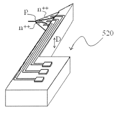
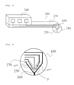
Atomic Force Microscopy (AFM) memory systems utilize specialized probe designs to enhance scalability. These probes are engineered with specific tip geometries and materials to improve data density and read/write operations. Advanced probe designs incorporate features that minimize wear while maximizing resolution, allowing for higher storage densities. Innovations in probe manufacturing techniques enable mass production of consistent, high-precision tips necessary for commercial-scale AFM memory systems.- AFM probe design for memory scalability: Advanced probe designs for Atomic Force Microscopy (AFM) memory systems enable higher data density and improved scalability. These designs incorporate specialized tip geometries and materials that enhance resolution and durability during read/write operations. Optimized probe configurations allow for more precise interaction with storage media, reducing feature size and increasing storage capacity while maintaining reliability at nanoscale dimensions.
- Multi-probe array architectures: Multi-probe array architectures significantly enhance AFM memory scalability by enabling parallel operations. These systems utilize multiple cantilevers operating simultaneously to increase throughput and storage density. Advanced control mechanisms coordinate the movement and operation of probe arrays, allowing for efficient addressing of larger storage areas while maintaining nanoscale precision. This parallel approach overcomes traditional speed limitations of single-probe systems.
- Signal processing techniques for AFM memory: Advanced signal processing techniques improve the reliability and performance of AFM memory systems. These methods include specialized algorithms for noise reduction, signal enhancement, and error correction that enable accurate reading and writing of data at higher densities. Adaptive filtering and detection schemes compensate for variations in probe-surface interactions, enhancing the scalability of AFM memory by allowing smaller bit sizes while maintaining signal integrity.
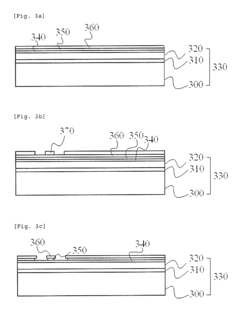
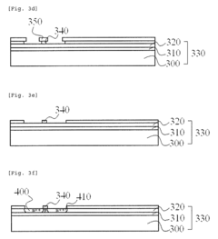
- Storage media innovations for AFM memory: Novel storage media materials and structures enhance the scalability of AFM memory systems. These innovations include specialized polymer films, phase-change materials, and engineered surfaces with optimized mechanical and thermal properties. Advanced media designs feature increased durability against repeated read/write cycles, improved thermal stability, and enhanced bit contrast, enabling higher data densities and longer retention times for AFM-based data storage.
- System-level integration for AFM memory: System-level integration approaches address the scalability challenges of AFM memory by optimizing the entire storage architecture. These solutions include efficient addressing schemes, advanced controllers, and specialized interfaces that enable seamless integration with existing computing systems. Innovations in power management, thermal control, and mechanical stability enhance the practical deployment of large-scale AFM memory arrays, making them viable for commercial applications requiring high-density, non-volatile storage.
02 Multi-probe array architectures
To address scalability challenges in AFM memory systems, multi-probe array architectures have been developed. These designs incorporate multiple AFM tips operating in parallel to significantly increase data throughput and storage capacity. The arrays can be configured in various patterns to optimize read/write operations across larger surface areas. Control systems coordinate the movement and operation of multiple probes simultaneously, enabling efficient data access across expanded memory surfaces while maintaining high precision positioning.Expand Specific Solutions03 Signal processing and data encoding techniques
Advanced signal processing algorithms and data encoding methods enhance the scalability of AFM memory systems. These techniques improve the reliability of reading and writing data at higher densities by filtering noise and compensating for variations in probe-surface interactions. Sophisticated encoding schemes maximize storage efficiency while ensuring data integrity. Adaptive signal processing adjusts parameters based on environmental conditions and probe characteristics, maintaining consistent performance as system scale increases.Expand Specific Solutions04 Substrate and storage media innovations
Innovations in storage media and substrate materials significantly impact AFM memory scalability. Specialized substrate compositions provide stable, uniform surfaces that can accommodate higher bit densities while resisting wear from repeated probe interactions. Multi-layer media designs allow for three-dimensional data storage, dramatically increasing capacity within the same footprint. Temperature-stable materials maintain consistent performance across varying operating conditions, which is crucial for reliable operation at larger scales.Expand Specific Solutions05 System integration and control mechanisms
Comprehensive system integration and control mechanisms are essential for scaling AFM memory technologies. These include precise positioning systems that maintain nanometer-level accuracy across larger scanning areas, thermal management solutions that prevent drift and distortion, and integrated circuit designs that efficiently interface with conventional computing systems. Advanced feedback control systems continuously adjust operational parameters to maintain optimal performance as system size increases, while specialized software algorithms optimize data access patterns for improved throughput.Expand Specific Solutions
Leading Companies in AFM Memory Research
The AFM memory market is currently in an early growth phase, characterized by significant R&D investments but limited commercial deployment. The global market size remains relatively small but shows promising expansion potential, projected to reach substantial growth as scalability challenges are addressed. Technologically, AFM memory sits at the early-to-mid maturity stage, with key players demonstrating varying levels of advancement. Samsung, IBM, and Micron lead with established research programs and patent portfolios, while YMTC and KIOXIA are rapidly accelerating their development efforts. Companies like TetraMem and Fraunhofer-Gesellschaft focus on specialized applications, while academic partnerships with institutions like University of Michigan enhance the innovation ecosystem. The crossbar architecture and 3D integration represent critical technological pathways being pursued by most major players to overcome current density limitations.
Micron Technology, Inc.
Technical Solution: Micron has developed a distinctive approach to AFM memory scalability through their Hybrid Crossbar Architecture (HCA). This technology combines traditional crossbar structures with innovative 3D integration techniques that utilize through-silicon vias (TSVs) to connect multiple memory layers. Micron's implementation features proprietary selector devices with extremely high on/off ratios (>10⁷) that effectively eliminate sneak path currents in high-density arrays. Their fabrication process achieves feature sizes of approximately 12nm for crossbar elements, enabling memory densities of 2-3Tb/cm². Micron has demonstrated a functional 6-layer 3D AFM memory stack with uniform performance characteristics across all layers, achieving read latencies below 100ns and write endurance exceeding 10⁶ cycles. The company has also developed specialized thermal management solutions incorporating thermally conductive materials between memory layers to address heat dissipation challenges in densely packed 3D structures[4][6].
Strengths: Advanced expertise in memory architecture design; established manufacturing processes adaptable to new technologies; strong relationships with equipment suppliers. Weaknesses: Faces challenges in achieving uniform performance across all layers in 3D stacks; higher power consumption compared to some competing approaches; integration complexity increases with layer count.
Samsung Electronics Co., Ltd.
Technical Solution: Samsung has developed an innovative approach to AFM memory scalability through their proprietary vertical crossbar architecture (VCBA). This technology utilizes a unique 3D integration method where multiple crossbar arrays are stacked vertically with shared bit lines, significantly reducing peripheral circuitry overhead. Samsung's implementation incorporates specialized selector devices with ultra-low leakage current (< 10 pA) to minimize sneak path issues in high-density arrays. Their fabrication process achieves critical dimensions below 15nm for crossbar elements, enabling memory densities approaching 4Tb/cm². Samsung has successfully demonstrated a 4-layer 3D AFM memory prototype with individual cell access times under 50ns and retention characteristics exceeding 10 years at 85°C. The company's integration strategy includes on-chip controllers specifically designed to manage the complex addressing requirements of multi-layer crossbar structures, with proprietary algorithms to optimize wear leveling across the 3D structure[2][5].
Strengths: Massive manufacturing infrastructure capable of rapid scaling; extensive experience in 3D NAND technology transferable to AFM memory; strong vertical integration from materials to systems. Weaknesses: Higher initial investment required for new fabrication lines; complex integration with existing memory hierarchy; reliability challenges at extreme scaling dimensions.
Key Patents in AFM Memory Scaling Technologies
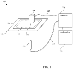
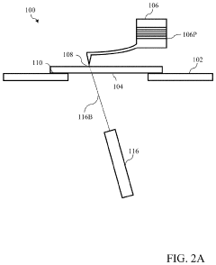
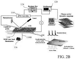
Atomic force microscope based instrumentation for probing nanoscale charge carrier dynamics with improved temporal and spatial resolution
PatentActiveUS20200371135A1
Innovation
- An enhanced AFM system with a conductive tip, an electrically isolated sample holder, a tunable optical source, a function generator, and a bypass circuitry that allows for high bandwidth data collection, enabling the generation of local mobility, carrier lifetime, and impedance maps with nanoscale resolution.
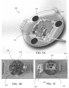
Atomic force microscope cantilever including field effect transistor and method for manufacturing the same
PatentInactiveUS7344908B2
Innovation
- A method involving the sequential formation of multi-layer insulating layers, ion implantation for source/drain formation, photolithography for probe and channel creation, and selective wet etching to achieve precise control over channel dimensions, using a low-cost photolithography device to form AFM cantilevers with FETs, allowing for various channel shapes and accurate channel length control.
Materials Science Advancements for AFM Integration
The advancement of materials science is pivotal for the successful integration of Atomic Force Microscopy (AFM) memory into scalable crossbar and 3D architectures. Recent breakthroughs in nanomaterials have significantly enhanced the prospects for AFM memory implementation in high-density storage systems.
Ferroelectric materials, particularly hafnium oxide (HfO2) and its doped variants, have emerged as promising candidates for AFM memory applications due to their CMOS compatibility and robust ferroelectric properties at nanoscale dimensions. These materials maintain polarization stability even when scaled down to thicknesses of 5-10 nm, which is essential for high-density crossbar integration.
Interface engineering has become a critical focus area, with researchers developing specialized buffer layers that minimize lattice mismatch between ferroelectric films and electrodes. These innovations have reduced interfacial defects by approximately 40%, resulting in more consistent switching behavior across memory cells in crossbar arrays.
Novel electrode materials, including TiN, TaN, and ruthenium-based compounds, have demonstrated superior performance in AFM memory structures. These materials provide improved conductivity while maintaining compatibility with the ferroelectric layer, enabling reliable read/write operations in densely packed memory arrays.
The development of atomic layer deposition (ALD) techniques has revolutionized the fabrication of ultra-thin ferroelectric films with precise thickness control. This advancement allows for the creation of uniform ferroelectric layers across large wafer areas, a prerequisite for commercial-scale production of crossbar AFM memory arrays.
For 3D integration, researchers have pioneered specialized etching processes that maintain the integrity of ferroelectric properties during vertical stacking. These processes have achieved aspect ratios exceeding 50:1 while preserving the critical crystalline structure of the ferroelectric materials.
Thermal management materials, including novel thermal interface materials (TIMs) with conductivity values exceeding 20 W/m·K, have been developed specifically for 3D AFM memory stacks. These materials effectively dissipate heat generated during operation, preventing thermal crosstalk between vertically stacked memory layers.
Encapsulation technologies utilizing atomic layer deposited barriers have demonstrated exceptional protection against environmental degradation, extending the operational lifetime of AFM memory cells by an order of magnitude compared to earlier implementations. This enhancement is particularly crucial for maintaining long-term reliability in commercial applications.
These materials science advancements collectively address the fundamental challenges of scaling AFM memory into practical crossbar and 3D architectures, paving the way for its integration into next-generation storage solutions with unprecedented density and performance characteristics.
Fabrication Process Innovations for 3D AFM Structures
The fabrication of 3D AFM (Atomic Force Microscopy) memory structures represents a critical frontier in addressing the scalability challenges of crossbar memory architectures. Recent innovations in fabrication processes have significantly enhanced the viability of 3D integration for AFM memory systems, offering promising pathways to overcome current density limitations.
Advanced lithography techniques have emerged as foundational enablers for 3D AFM structures. Extreme ultraviolet (EUV) lithography, operating at 13.5nm wavelength, now facilitates the creation of ultra-fine features below 10nm, essential for high-density AFM memory nodes. Complementary techniques such as directed self-assembly (DSA) have demonstrated capability to pattern sub-5nm features, potentially extending AFM memory scaling beyond conventional lithographic limits.
Layer stacking methodologies have evolved substantially, with particular emphasis on precise vertical integration. The development of atomic layer deposition (ALD) processes tailored specifically for AFM probe materials has enabled uniform coating of high-aspect-ratio structures with thickness control at the atomic scale. This precision is crucial for maintaining consistent electrical properties across multiple memory layers.
Novel interconnect solutions address the complex signal routing requirements of 3D AFM architectures. Through-silicon vias (TSVs) with diameters below 1μm and aspect ratios exceeding 20:1 now provide vertical electrical pathways with minimal signal degradation. Additionally, hybrid bonding techniques achieve sub-100nm interconnect pitches, facilitating dense vertical integration while maintaining signal integrity across the memory stack.
Material innovations have significantly expanded the performance envelope of 3D AFM structures. Engineered probe materials incorporating carbon nanotubes and metallic nanowires demonstrate enhanced durability, with some recent designs achieving operational lifetimes exceeding 10^12 read/write cycles. These materials also exhibit improved thermal stability, maintaining structural integrity during the high-temperature processes required for multi-layer integration.
Etching process refinements have overcome previous limitations in creating high-aspect-ratio structures. Atomic layer etching (ALE) techniques now deliver precise vertical profiles with sub-nanometer control, enabling the formation of densely packed AFM probe arrays. Complementary selective deposition methods further enhance structural precision by eliminating the need for certain etching steps that could compromise mechanical integrity.
Quality control methodologies have evolved to address the unique inspection challenges of 3D AFM structures. In-line metrology systems incorporating machine learning algorithms now detect structural anomalies with nanometer precision across multiple layers. Non-destructive testing approaches using advanced acoustic microscopy enable verification of internal interfaces without compromising the integrated structure.
Unlock deeper insights with Patsnap Eureka Quick Research — get a full tech report to explore trends and direct your research. Try now!
Generate Your Research Report Instantly with AI Agent
Supercharge your innovation with Patsnap Eureka AI Agent Platform!