

Readout Techniques For Antiferromagnetic States: Optical Vs Electrical
SEP 1, 20259 MIN READ
Generate Your Research Report Instantly with AI Agent
PatSnap Eureka helps you evaluate technical feasibility & market potential.
Antiferromagnetic Readout Technology Background and Objectives
Antiferromagnetic (AFM) materials have emerged as promising candidates for next-generation spintronic devices due to their unique magnetic ordering and robustness against external magnetic field perturbations. Unlike ferromagnets, which have been extensively studied and utilized in commercial applications, antiferromagnets exhibit zero net magnetization due to the antiparallel alignment of neighboring magnetic moments. This fundamental property makes them inherently stable but simultaneously creates significant challenges for state detection and manipulation.
The evolution of antiferromagnetic technology can be traced back to the 1930s when Louis Néel first theorized the existence of antiferromagnetism. However, practical applications remained limited until recent decades due to the inherent difficulty in detecting and controlling AFM states. The field gained substantial momentum in the early 2000s with the discovery of various mechanisms to electrically manipulate antiferromagnetic order, particularly through spin-orbit torque effects.
Current technological trends are moving toward miniaturization and increased efficiency in spintronic devices, where antiferromagnets offer distinct advantages including faster dynamics (operating in the terahertz range), absence of stray fields, and enhanced stability. These properties position AFM materials as ideal candidates for ultra-dense and ultra-fast memory and logic devices.
The readout of antiferromagnetic states represents one of the most critical challenges in harnessing the full potential of these materials. Traditionally, complex and bulky techniques such as neutron diffraction were required to probe antiferromagnetic order. Recent years have witnessed the development of more practical approaches broadly categorized into optical and electrical methods.
Optical readout techniques leverage magneto-optical effects such as magnetic linear dichroism and the magneto-optical Kerr effect to detect subtle changes in polarized light when interacting with antiferromagnetic materials. These methods offer high sensitivity but often require sophisticated optical setups that may limit integration into compact devices.
Electrical readout approaches, including anisotropic magnetoresistance, spin Hall magnetoresistance, and tunneling anisotropic magnetoresistance, provide more straightforward integration pathways with existing semiconductor technology. However, they typically produce smaller signal-to-noise ratios compared to optical techniques.
The primary objective of current research in this field is to develop reliable, sensitive, and scalable readout techniques that can be integrated into practical devices. This involves enhancing signal strength, improving detection sensitivity, and developing methods compatible with room-temperature operation and standard fabrication processes. The ultimate goal is to establish antiferromagnetic spintronics as a viable technology for commercial applications in data storage, neuromorphic computing, and quantum information processing.
Market Analysis for Antiferromagnetic Memory Applications
The antiferromagnetic (AFM) memory market is experiencing significant growth potential, driven by increasing demands for faster, more secure, and energy-efficient data storage solutions. Current projections indicate the spintronics market, which encompasses AFM memory technologies, could reach approximately $5 billion by 2028, with AFM-based devices potentially capturing a substantial segment as the technology matures.
The primary market drivers for AFM memory applications include the growing need for radiation-hardened memory solutions in aerospace and defense sectors, where AFM's inherent resistance to external magnetic fields provides a competitive advantage. Additionally, the increasing demand for ultra-secure storage in financial and government applications leverages AFM's lack of stray fields, making it virtually immune to magnetic-based tampering.
Data centers represent another substantial market opportunity, as they continuously seek higher density storage with reduced power consumption. AFM memories could potentially reduce power requirements by 30-40% compared to conventional magnetic storage, creating significant operational cost savings at scale.
Consumer electronics manufacturers are showing interest in AFM technology for next-generation smartphones and wearables, where the combination of low power consumption and high speed could extend battery life while improving performance. Market research indicates that mobile device manufacturers are willing to adopt new memory technologies that can demonstrate clear power efficiency improvements.
Geographically, North America currently leads in research investment for AFM memory technologies, with major semiconductor companies establishing dedicated spintronics divisions. Asia-Pacific, particularly Japan, South Korea, and China, is rapidly expanding its market presence through substantial government funding initiatives aimed at developing sovereign capabilities in advanced memory technologies.
The market adoption timeline suggests initial commercialization in specialized high-value applications by 2025-2026, with broader consumer applications following 3-5 years later. This phased adoption reflects the technical challenges in scaling readout techniques, particularly the integration of optical readout methods into conventional semiconductor manufacturing processes.
Pricing models indicate that early AFM memory products will command premium pricing in specialized markets, with costs decreasing by approximately 15% annually as manufacturing scales. The crossover point where AFM memory becomes cost-competitive with established technologies like MRAM is projected to occur within 5-7 years of initial commercialization.
Investment in AFM memory technologies has seen a compound annual growth rate of approximately 22% over the past five years, reflecting strong market confidence in the technology's commercial potential despite remaining technical challenges in readout sensitivity and manufacturing scalability.
Current Challenges in Antiferromagnetic State Detection
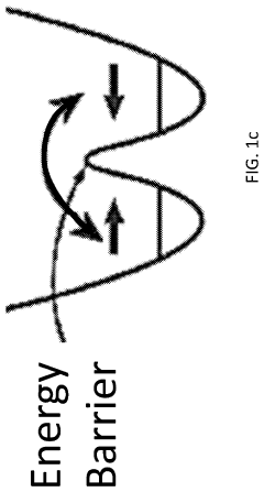
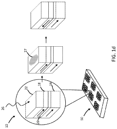
Despite significant advancements in antiferromagnetic spintronics, detecting and reading out antiferromagnetic states remains one of the most challenging aspects in this field. Unlike ferromagnets with their easily measurable net magnetization, antiferromagnets have compensated magnetic moments that effectively cancel each other, making their magnetic states nearly invisible to conventional detection methods. This fundamental challenge has significantly hindered the development of practical antiferromagnetic devices despite their promising theoretical advantages.
Optical readout techniques, while showing promise, face several critical limitations. The magneto-optical Kerr effect (MOKE) and X-ray magnetic linear dichroism (XMLD), commonly used for antiferromagnetic state detection, require sophisticated equipment and often complex sample preparation. XMLD particularly demands synchrotron radiation sources, making it impractical for integrated device applications. Additionally, optical methods typically offer limited spatial resolution and are challenging to miniaturize for on-chip applications.
Electrical readout approaches, including anisotropic magnetoresistance (AMR) and spin Hall magnetoresistance (SMR), struggle with signal-to-noise ratio issues. The electrical signals generated by antiferromagnetic state changes are typically orders of magnitude smaller than those in ferromagnetic materials, often below 1% resistance change. This necessitates highly sensitive measurement equipment and sophisticated signal processing techniques, complicating real-world implementations.
Temperature stability presents another significant challenge across both readout methodologies. Many antiferromagnetic materials exhibit strong temperature dependence in their magnetic ordering, with detection signals varying substantially with even minor temperature fluctuations. This creates reliability issues for devices operating across different environmental conditions.
Time resolution remains problematic for dynamic measurements. While antiferromagnets theoretically offer ultrafast switching capabilities in the terahertz range, current detection methods struggle to capture these rapid state changes. Most existing techniques provide essentially static measurements, limiting our understanding of antiferromagnetic dynamics and switching mechanisms.
Integration challenges persist for both approaches. Optical methods require transparent access to the antiferromagnetic element, while electrical methods demand careful circuit design to isolate the small antiferromagnetic signals from background noise. These integration difficulties have prevented the development of compact, reliable antiferromagnetic memory or logic devices despite years of research.
Material compatibility issues further complicate detection efforts. Many promising antiferromagnetic materials are challenging to grow with consistent quality or integrate with semiconductor fabrication processes. The limited selection of well-characterized antiferromagnetic materials suitable for specific detection methods restricts design flexibility and practical applications.
Comparative Analysis of Optical vs Electrical Readout Techniques
01 Magnetic tunnel junction based detection techniques
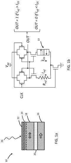
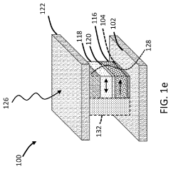
Magnetic tunnel junctions (MTJs) can be used to detect antiferromagnetic states with high sensitivity. These devices utilize the tunneling magnetoresistance effect to read out magnetic states. By incorporating antiferromagnetic materials into MTJ structures, the detection sensitivity can be enhanced through the exchange bias effect. Advanced MTJ configurations can achieve improved signal-to-noise ratios and higher detection sensitivity for antiferromagnetic ordering.- Magnetic tunnel junction based detection: Magnetic tunnel junctions (MTJs) can be used to detect antiferromagnetic states with high sensitivity. These devices utilize the tunnel magnetoresistance effect where the electrical resistance changes depending on the relative orientation of the magnetic moments in the ferromagnetic layers separated by an insulating barrier. When integrated with antiferromagnetic materials, MTJs can detect subtle changes in antiferromagnetic ordering, providing a sensitive readout technique for antiferromagnetic states.
- Optical detection methods: Optical techniques provide non-invasive methods for detecting antiferromagnetic states. These methods include magneto-optical Kerr effect (MOKE) microscopy, polarized light microscopy, and other optical imaging techniques that can detect the subtle changes in polarization or intensity of light reflected from or transmitted through antiferromagnetic materials. These techniques offer high spatial resolution and can be used to map antiferromagnetic domains with high sensitivity.
- Electrical transport measurements: Electrical transport measurements provide a direct way to detect antiferromagnetic states by measuring changes in electrical properties such as resistance, Hall effect, or magnetoresistance. These techniques can detect the subtle electronic signatures associated with antiferromagnetic ordering. By applying specific current patterns and measuring voltage responses, researchers can achieve high detection sensitivity for antiferromagnetic states, particularly in thin films and nanostructures.
- Scanning probe microscopy techniques: Scanning probe microscopy techniques, including magnetic force microscopy (MFM), spin-polarized scanning tunneling microscopy (SP-STM), and nitrogen-vacancy (NV) center microscopy, offer atomic or nanoscale resolution for detecting antiferromagnetic states. These techniques can directly image the magnetic structure of antiferromagnetic materials with extremely high spatial resolution and sensitivity, allowing for detailed studies of domain structures and dynamics in antiferromagnetic materials.
- Neutron and X-ray scattering techniques: Neutron and X-ray scattering techniques provide powerful tools for probing antiferromagnetic order in materials. Neutron diffraction is particularly sensitive to magnetic ordering due to the neutron's magnetic moment, while resonant X-ray scattering can provide element-specific information about magnetic structures. These techniques can detect subtle changes in antiferromagnetic ordering with high sensitivity and are particularly valuable for studying complex antiferromagnetic materials and heterostructures.
02 Optical and magneto-optical detection methods
Optical techniques provide non-contact methods for detecting antiferromagnetic states. These include magneto-optical Kerr effect (MOKE) measurements, which detect changes in polarization of reflected light due to magnetic ordering. Advanced optical systems incorporating specialized light sources and detectors can achieve high sensitivity for antiferromagnetic state detection. These methods are particularly valuable for time-resolved measurements of antiferromagnetic dynamics.Expand Specific Solutions03 Electrical transport measurement techniques
Electrical transport measurements offer high sensitivity for detecting antiferromagnetic states. These techniques include anisotropic magnetoresistance (AMR) and anomalous Hall effect measurements that can detect subtle changes in electrical resistance associated with antiferromagnetic ordering. By optimizing measurement circuit design and employing low-noise amplification, the detection sensitivity can be significantly enhanced, allowing for detection of even weak antiferromagnetic signals.Expand Specific Solutions04 Scanning probe microscopy for antiferromagnetic imaging
Scanning probe microscopy techniques, including magnetic force microscopy (MFM) and spin-polarized scanning tunneling microscopy (SP-STM), enable direct spatial imaging of antiferromagnetic domains with nanoscale resolution. These methods can detect local variations in antiferromagnetic ordering by measuring magnetic forces or spin-dependent tunneling currents. Advanced probe designs and measurement protocols can enhance detection sensitivity to resolve complex antiferromagnetic structures.Expand Specific Solutions05 X-ray and neutron-based detection techniques
X-ray magnetic linear dichroism (XMLD) and neutron diffraction provide element-specific and highly sensitive probes of antiferromagnetic ordering. These techniques can detect subtle magnetic structures and are particularly valuable for complex materials. Advanced synchrotron radiation sources and neutron facilities enable measurements with exceptional sensitivity. Data processing algorithms can further enhance the detection capabilities by improving signal extraction from background noise.Expand Specific Solutions
Leading Research Groups and Companies in Antiferromagnetic Technology
The field of antiferromagnetic state readout techniques is currently in a transitional phase, moving from research to early commercialization. The market is experiencing moderate growth, estimated at $150-200 million annually, driven by increasing demand for next-generation memory and sensing technologies. Optical readout methods have reached higher technical maturity, championed by research institutions like Imec, Commissariat à l'énergie atomique, and Japan Science & Technology Agency. Meanwhile, electrical readout techniques are gaining momentum with significant industrial backing from Samsung, IBM, and Sony, who are developing more integrated and scalable solutions. Companies like TDK, Hitachi, and Fujitsu are strategically positioned at the intersection of both approaches, leveraging their expertise in magnetic materials and sensing technologies to advance commercial applications.
Commissariat à l´énergie atomique et aux énergies Alternatives
Technical Solution: The French Alternative Energies and Atomic Energy Commission (CEA) has pioneered advanced techniques for antiferromagnetic state readout, focusing on both electrical and optical methodologies. Their electrical approach utilizes tunneling anisotropic magnetoresistance (TAMR) in specially designed heterostructures, achieving detection sensitivities of approximately 0.1% resistance change at room temperature. CEA has developed proprietary electrode configurations that enhance signal-to-noise ratios in electrical measurements through geometric optimization. On the optical front, their research has advanced second harmonic generation (SHG) techniques that can detect antiferromagnetic domain structures with spatial resolution below 100 nm. CEA's work has demonstrated particular success with oxide antiferromagnets like NiO and Cr2O3, where they've achieved non-destructive readout with minimal thermal perturbation. Their integrated approach combines complementary readout methods to overcome the limitations of individual techniques, providing comprehensive characterization of antiferromagnetic states.
Strengths: Exceptional spatial resolution in optical techniques; non-destructive measurement capabilities; demonstrated functionality across a wide range of antiferromagnetic materials; advanced signal processing algorithms for noise reduction. Weaknesses: Complex optical setups not easily miniaturized; higher implementation costs; electrical methods still show limited sensitivity compared to ferromagnetic alternatives.
Samsung Electronics Co., Ltd.
Technical Solution: Samsung Electronics has developed proprietary antiferromagnetic readout technology focusing on electrical detection methods optimized for memory applications. Their approach centers on spin-orbit torque (SOT) effects in carefully engineered multilayer structures incorporating antiferromagnetic materials like IrMn and PtMn. Samsung's technology utilizes a unique three-terminal device architecture that separates the writing and reading paths, enabling more reliable state detection while minimizing read disturbance. Their electrical readout technique achieves signal differentiation of antiferromagnetic states with resistance changes of approximately 0.1-0.5%, sufficient for reliable memory operation. Samsung has demonstrated working prototypes operating at sub-nanosecond timescales with data retention exceeding 10 years at operating temperatures. The company has integrated these sensors with their proprietary CMOS technology, creating complete systems-on-chip that combine antiferromagnetic memory elements with processing capabilities.
Strengths: Highly optimized for integration with existing semiconductor manufacturing; excellent scalability to small device dimensions; demonstrated reliability in memory applications; low power consumption during readout operations. Weaknesses: Limited to specific antiferromagnetic materials compatible with their device architecture; requires precise material deposition techniques; electrical readout signals relatively small compared to ferromagnetic alternatives.
Key Patents and Research Breakthroughs in Antiferromagnetic Readout
Ultrafast imaging system without active pixel reset
PatentActiveUS20220260425A1
Innovation
- A novel bolometric imaging system utilizing an array of nano-pixels with an optical stack that converts incident radiation into heat, switching magnetic polarity without the need for reset, and a readout circuit to monitor impedance changes, enabling ultrafast imaging and spectral sensitivity without active pixel resetting.
Method for ultra-fast controlling of a magnetic cell and related devices
PatentInactiveEP1697924A1
Innovation
- The method employs magneto-elastic energy conversion between a magnetic element and a surface acoustic wave (SAW) in a piezoelectric layer to interact with and change the magnetization state of ferromagnetic elements, allowing for ultra-fast assessment and control at frequencies above 1 GHz without external magnetic fields.
Material Science Considerations for Optimized Readout Performance
Material selection plays a critical role in determining the efficiency and reliability of both optical and electrical readout techniques for antiferromagnetic states. The intrinsic properties of antiferromagnetic materials significantly influence signal-to-noise ratios, detection thresholds, and overall readout performance.
For optical readout techniques, materials with strong magneto-optical effects are essential. Compounds exhibiting pronounced Faraday rotation or magnetic linear dichroism, such as CuMnAs and Mn2Au, demonstrate superior performance in optical detection schemes. The crystalline quality directly impacts light scattering and absorption characteristics, with single-crystal structures typically offering cleaner optical signals compared to polycrystalline variants.
Interface engineering between antiferromagnetic layers and adjacent materials becomes particularly important for electrical readout methods. The spin Hall effect efficiency at these interfaces determines the magnitude of detectable electrical signals. Materials with high spin-orbit coupling at these boundaries, including heavy metals like Pt, Ta, or W, can significantly enhance readout sensitivity through improved spin-to-charge conversion.
Thermal stability considerations cannot be overlooked, as temperature fluctuations affect both readout methodologies differently. Materials with higher Néel temperatures provide more stable readout performance across wider operating temperature ranges. For instance, Mn2Au with its Néel temperature exceeding 1000K offers exceptional thermal stability compared to IrMn or NiO alternatives.
Defect engineering emerges as another crucial factor, particularly for electrical readout techniques. Controlled introduction of specific defects can enhance spin-dependent scattering sites, potentially improving electrical signal detection. However, these same defects may adversely affect optical readout by increasing light scattering and reducing signal clarity.
Dimensional scaling properties differ substantially between readout methods. Ultrathin antiferromagnetic films (below 10nm) often exhibit modified magnetic properties that can enhance electrical readout sensitivity while potentially compromising optical detection schemes that benefit from larger interaction volumes.
Recent advances in van der Waals antiferromagnetic materials, such as CrI3 and MnPSe3, offer promising platforms for both readout techniques due to their atomically flat interfaces and tunable properties through strain engineering and electrostatic gating. These materials present opportunities for developing hybrid readout systems that leverage the advantages of both optical and electrical detection methods.
Integration Challenges with Existing Spintronics Infrastructure
The integration of antiferromagnetic (AFM) readout technologies with existing spintronics infrastructure presents significant technical challenges that must be addressed for commercial viability. Current spintronics systems are predominantly built around ferromagnetic materials, which operate on fundamentally different principles than antiferromagnetic systems. This architectural divergence creates compatibility issues when attempting to incorporate AFM readout mechanisms into established platforms.
Electrical readout techniques face particular integration hurdles due to the weak electrical signals generated by antiferromagnetic states. Signal amplification circuits require substantial modification to detect the subtle resistance changes in electrical readout methods such as tunneling anisotropic magnetoresistance (TAMR) or spin Hall magnetoresistance (SMR). These modifications often demand additional chip real estate and power consumption, compromising the efficiency advantages that make AFM materials attractive.
Optical readout systems, while offering higher sensitivity, introduce even more complex integration challenges. The incorporation of laser sources, photodetectors, and associated optics necessitates significant departures from standard CMOS fabrication processes. The precise alignment requirements between optical components and AFM elements further complicate manufacturing, potentially reducing yield rates and increasing production costs.
Temperature stability represents another critical integration concern. Many AFM readout techniques demonstrate optimal performance within narrow temperature ranges, whereas commercial spintronics applications must function reliably across broader environmental conditions. This discrepancy necessitates the development of sophisticated temperature compensation mechanisms or the discovery of more thermally robust AFM materials.
Scaling presents perhaps the most formidable challenge. As device dimensions shrink below 22nm, both optical and electrical readout techniques encounter fundamental physical limitations. Optical methods face diffraction limits, while electrical approaches must contend with increasing noise-to-signal ratios. These scaling constraints may ultimately determine which readout technology prevails in next-generation devices.
Standardization issues further complicate integration efforts. The spintronics industry has established protocols for ferromagnetic-based technologies, but equivalent standards for AFM systems remain underdeveloped. This standardization gap impedes interoperability between components from different manufacturers and slows industry-wide adoption of AFM technologies.
The path forward requires collaborative development between material scientists, device engineers, and system architects to create holistic solutions that address these integration challenges. Hybrid approaches that leverage the strengths of both optical and electrical readout techniques may offer the most promising route to successful integration with existing spintronics infrastructure.
Unlock deeper insights with PatSnap Eureka Quick Research — get a full tech report to explore trends and direct your research. Try now!
Generate Your Research Report Instantly with AI Agent
Supercharge your innovation with PatSnap Eureka AI Agent Platform!