Optimizing Film Thickness And Strain For Performance Gains
SEP 1, 20259 MIN READ
Generate Your Research Report Instantly with AI Agent
Patsnap Eureka helps you evaluate technical feasibility & market potential.
Film Thickness Technology Background and Objectives
The evolution of thin film technology has been a cornerstone of semiconductor and microelectronics advancement since the mid-20th century. Initially developed for basic electronic components, thin film technology has progressively expanded into diverse applications including integrated circuits, optical coatings, solar cells, and more recently, flexible electronics and biomedical devices. The optimization of film thickness and strain represents a critical frontier in enhancing device performance across these applications.
Film thickness optimization has historically been driven by the semiconductor industry's pursuit of Moore's Law, requiring increasingly thinner films to achieve higher component densities. Early films measured in micrometers, while today's advanced processes routinely work with films of just a few nanometers. This dramatic reduction has enabled exponential improvements in computational power but has simultaneously introduced significant engineering challenges related to uniformity, defect management, and strain control.
Strain engineering emerged as a complementary technique in the early 2000s when researchers discovered that controlled strain in semiconductor films could significantly enhance carrier mobility. Intel's 90nm process technology in 2003 marked one of the first commercial implementations of strained silicon, demonstrating performance gains of up to 30% without requiring dimensional scaling. This breakthrough established strain as a fundamental parameter alongside thickness in film optimization strategies.
The relationship between film thickness and strain follows complex physical principles governed by lattice mismatch, thermal expansion differences, and growth conditions. As films become thinner, their mechanical properties increasingly deviate from bulk behavior, creating both challenges and opportunities for performance engineering. Ultra-thin films often exhibit quantum confinement effects that can be exploited for novel electronic and optical properties.
Current technological objectives focus on developing precise control methodologies for simultaneously optimizing thickness and strain parameters. This includes advancing deposition techniques such as Atomic Layer Deposition (ALD) and Molecular Beam Epitaxy (MBE) that offer atomic-level precision, as well as in-situ characterization tools capable of real-time monitoring during fabrication processes.
The ultimate goal of this technological pursuit is to enable next-generation devices with enhanced performance metrics including higher speeds, lower power consumption, improved reliability, and novel functionalities. Additionally, there is growing interest in extending these optimization techniques to emerging materials beyond traditional semiconductors, including two-dimensional materials, complex oxides, and organic semiconductors, potentially opening new application domains and performance paradigms.
Market Applications and Demand Analysis
The market for thin film optimization technologies has experienced significant growth in recent years, driven primarily by the semiconductor industry's relentless pursuit of performance improvements. The global semiconductor market, where film thickness and strain engineering are critical, reached approximately $600 billion in 2023, with projections indicating continued expansion at a compound annual growth rate of 8-10% through 2030.
Demand for optimized film thickness and strain engineering solutions spans multiple high-value sectors. The semiconductor industry represents the largest market segment, where nanometer-scale control of film properties directly impacts transistor performance in logic and memory applications. Advanced nodes at 3nm and below require unprecedented precision in film deposition and strain management to achieve desired carrier mobility enhancements.
The display technology sector constitutes another substantial market, with OLED and microLED manufacturers seeking optimized thin film solutions to improve efficiency, color accuracy, and device longevity. This segment values strain engineering particularly for flexible and foldable display applications, where mechanical reliability under repeated deformation cycles is paramount.
Photovoltaic cell manufacturing represents a rapidly growing application area, with thin film optimization directly impacting energy conversion efficiency. Recent advancements in perovskite solar cells have heightened interest in precise film thickness control techniques, as variations of mere nanometers can significantly alter performance characteristics.
Market analysis reveals regional variations in demand patterns. East Asia dominates manufacturing capacity for semiconductor and display technologies, accounting for over 70% of global production facilities requiring advanced film optimization solutions. North America and Europe lead in research and development activities, particularly in emerging applications like quantum computing where strain engineering enables novel device functionalities.
Customer requirements across these markets consistently emphasize several key performance indicators: thickness uniformity across increasingly larger substrate sizes, strain predictability and reproducibility, compatibility with existing manufacturing processes, and cost-effectiveness at production scale. The ability to characterize and control film properties in-situ during manufacturing represents a particularly high-value capability with strong market demand.
Industry forecasts suggest accelerating demand for film optimization technologies that can address heterogeneous integration challenges, where dissimilar materials with mismatched lattice constants must function together in advanced packaging applications. This trend aligns with the broader industry movement toward chiplet-based architectures and three-dimensional integration strategies.
Current Challenges in Film Thickness and Strain Control
Despite significant advancements in thin film technology, the precise control of film thickness and strain remains one of the most challenging aspects in semiconductor manufacturing and materials science. Current deposition techniques such as Physical Vapor Deposition (PVD), Chemical Vapor Deposition (CVD), and Atomic Layer Deposition (ALD) each present unique limitations when optimizing for both thickness and strain parameters simultaneously.
The primary challenge lies in achieving nanometer-scale thickness uniformity across large wafer surfaces. Even state-of-the-art equipment struggles to maintain consistency below 5nm thickness, with edge effects and chamber geometry creating variations that can significantly impact device performance. These non-uniformities become increasingly problematic as device dimensions continue to shrink according to Moore's Law projections.
Strain engineering, while offering tremendous potential for performance enhancement, introduces additional complexity. The intentional introduction of strain to modify electronic band structures and carrier mobility must be precisely controlled. Current methods often result in strain gradients rather than uniform strain fields, creating unpredictable performance variations across devices. The relationship between deposition parameters and resultant strain profiles remains incompletely understood, particularly for novel material systems.
Temperature management during deposition represents another significant hurdle. Thermal expansion coefficient mismatches between substrate and film materials create unintended strain during cooling, which can lead to delamination, cracking, or performance degradation. Real-time monitoring systems lack the resolution to detect these issues during processing, forcing manufacturers to rely on post-deposition characterization and statistical process control.
Material interfaces present particular difficulties, as lattice mismatches between different layers create strain fields that propagate unpredictably. While this can be exploited beneficially in some applications, such as in strained silicon technology, controlling these effects precisely across large areas remains challenging. Interface engineering approaches using buffer layers or compositional grading add process complexity and cost.
Metrology limitations further compound these challenges. Current in-line measurement techniques struggle to simultaneously characterize both thickness and strain with the required precision. Techniques like X-ray diffraction provide accurate strain measurements but are typically too slow for production environments, while optical methods offer speed but lack strain sensitivity.
Finally, the industry faces significant knowledge gaps in multiscale modeling. Current simulation tools inadequately bridge atomic-scale phenomena with wafer-level effects, making it difficult to predict how process adjustments will affect final film properties. This forces manufacturers to rely heavily on empirical approaches, extending development cycles and increasing costs for new technology nodes.
Current Methodologies for Film Thickness Optimization
01 Measurement techniques for thin film thickness and strain
Various optical and non-optical techniques are used to measure thickness and strain in thin films. These include ellipsometry, interferometry, X-ray diffraction, and spectroscopic methods. These techniques allow for precise determination of film thickness down to nanometer scale and can detect strain variations across the film surface, which is crucial for quality control in semiconductor manufacturing and other thin film applications.- Measurement techniques for thin film thickness and strain: Various optical and non-optical techniques are used to measure thickness and strain in thin films. These include ellipsometry, interferometry, X-ray diffraction, and spectroscopic methods. These techniques allow for precise determination of film properties without damaging the sample, which is crucial for quality control in semiconductor manufacturing and other applications requiring thin film characterization.
- Strain management in semiconductor thin films: Managing strain in semiconductor thin films is essential for controlling electronic properties and preventing device failure. Techniques include buffer layer insertion, compositional grading, and post-deposition thermal treatments. Controlled strain can enhance carrier mobility in certain semiconductor devices, while unwanted strain can lead to defect formation and delamination issues.
- Thin film deposition methods and thickness control: Various deposition methods are employed to create thin films with precisely controlled thickness, including physical vapor deposition, chemical vapor deposition, atomic layer deposition, and sputtering. In-situ monitoring systems allow real-time control of film growth, enabling the production of films with specific thickness profiles and minimizing thickness variations across substrates.
- Relationship between thickness and strain in thin films: The relationship between film thickness and strain is complex and depends on material properties, substrate characteristics, and deposition conditions. Generally, thinner films can accommodate higher strain without relaxation through defect formation. Critical thickness thresholds exist beyond which strain relaxation occurs through mechanisms such as dislocation formation or film cracking. Understanding this relationship is crucial for designing stable multilayer structures.
- Strain engineering for device performance enhancement: Intentional strain engineering in thin films is used to enhance device performance in various applications. By carefully controlling strain states in semiconductor layers, carrier mobility can be significantly improved, leading to faster transistors. Strain engineering is also applied in optical films to modify bandgap properties and in MEMS devices to create specific mechanical responses. This approach has become essential in advanced microelectronics manufacturing.
02 Strain control in semiconductor thin films
Methods for controlling and manipulating strain in semiconductor thin films to enhance device performance. Strain engineering can modify electronic properties of materials, improving carrier mobility and electrical characteristics. Techniques include using buffer layers, lattice mismatched substrates, and post-deposition treatments to induce desired strain profiles in thin films for applications in transistors, LEDs, and other electronic devices.Expand Specific Solutions03 Relationship between thickness and strain in thin films
The fundamental relationship between film thickness and strain is explored, showing how strain typically increases as film thickness decreases below critical thresholds. This relationship affects mechanical stability, adhesion properties, and electrical performance of thin films. Understanding this correlation is essential for designing reliable thin film devices and predicting failure mechanisms such as cracking, delamination, or electrical degradation in various applications.Expand Specific Solutions04 Deposition methods affecting thin film thickness and strain
Various deposition techniques and their impact on resultant film thickness uniformity and strain characteristics. Methods such as physical vapor deposition, chemical vapor deposition, atomic layer deposition, and sputtering create different strain profiles and thickness variations. Process parameters including temperature, pressure, and deposition rate significantly influence the microstructure, crystallinity, and residual stress in the deposited films.Expand Specific Solutions05 In-situ monitoring and control of thin film thickness and strain
Real-time monitoring systems for measuring and controlling thin film thickness and strain during the deposition or manufacturing process. These systems employ various sensors and feedback mechanisms to adjust process parameters dynamically, ensuring consistent film properties. In-situ monitoring reduces manufacturing defects, improves yield, and enables precise control of film characteristics for advanced applications in microelectronics, optics, and protective coatings.Expand Specific Solutions
Leading Companies and Research Institutions
The film thickness and strain optimization market is currently in a growth phase, with increasing demand driven by semiconductor and electronics industries seeking performance enhancements. Major players like FUJIFILM, Toray Industries, and Nitto Denko are leading technological innovation through advanced material science capabilities. Japanese corporations dominate this landscape, with companies such as Konica Minolta, Sumitomo Chemical, and Murata Manufacturing contributing significant R&D. The technology maturity varies across applications, with established players like AGC and Tosoh offering mature solutions while newer entrants like GTA Semiconductor and Shanghai Fujia New Materials are developing emerging approaches. Academic institutions including University of Electronic Science & Technology of China and Beijing Jiaotong University provide research support advancing fundamental understanding of strain engineering and thin film optimization techniques.
FUJIFILM Corp.
Technical Solution: FUJIFILM has pioneered advanced thin film optimization technologies leveraging their extensive expertise in precision coating and film formation. Their approach to film thickness and strain engineering centers on their proprietary "Nano-Optimization Process" (NOP) that enables precise control of film morphology at the molecular level. This technology utilizes controlled solvent evaporation rates combined with specialized substrate treatments to induce predetermined strain patterns during film formation. FUJIFILM's process can achieve thickness control with precision of ±2nm across large areas while simultaneously engineering strain gradients that enhance optical, electrical, or mechanical properties depending on the application requirements. Their most advanced implementation incorporates AI-driven process control systems that continuously monitor and adjust deposition parameters to maintain optimal thickness-strain relationships throughout production runs. This has enabled the development of high-performance optical films with thickness variations below 0.5% across 1.5m widths, while maintaining engineered strain profiles that enhance light transmission by up to 15% compared to conventional films.
Strengths: Exceptional large-area uniformity control; established mass production capabilities; demonstrated performance improvements in optical applications; sophisticated AI-driven process control. Weaknesses: Higher capital equipment costs for implementation; more complex process validation requirements; limited effectiveness for extremely thin films below 20nm.
Murata Manufacturing Co. Ltd.
Technical Solution: Murata Manufacturing has developed advanced thin film optimization technologies specifically targeting electronic component applications. Their approach focuses on precision control of both thickness and strain in functional ceramic and metal films used in capacitors, inductors, and RF components. Murata's "Nano-Precision Deposition" (NPD) technology enables thickness control with accuracy better than ±0.8nm while simultaneously engineering strain states to enhance electrical properties. Their process incorporates proprietary plasma-enhanced deposition techniques with real-time ellipsometry monitoring that provides continuous feedback for process adjustment. A distinctive feature of Murata's technology is their ability to create controlled strain gradients across film thickness, which has been shown to enhance dielectric constants in ceramic films by up to 20% compared to unstrained equivalents. For magnetic films used in inductors, Murata has demonstrated that optimized strain engineering can improve permeability by 15-25% while maintaining low hysteresis losses. Their manufacturing process has been successfully scaled to high-volume production, with demonstrated capability to maintain thickness uniformity better than 1% across thousands of components in batch processing.
Strengths: Highly optimized for electronic component applications; proven high-volume manufacturing capability; demonstrated significant performance improvements in electrical properties; excellent batch-to-batch consistency. Weaknesses: Limited application outside electronic components; higher capital equipment requirements; more complex process qualification procedures; challenges in adapting to very large substrate areas.
Key Technical Innovations in Strain Engineering
Process for producing semiconductor device, apparatus for optimizing film thickness, and process for optimizing film thickness
PatentInactiveUS6218313B1
Innovation
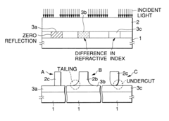
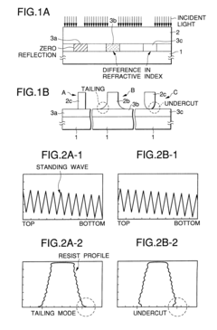
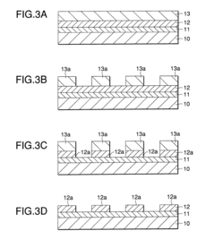
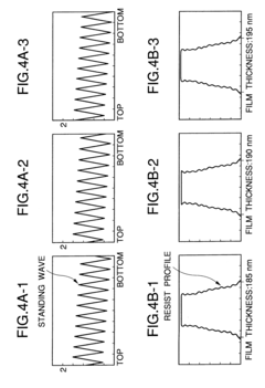
- A process and apparatus that simulate light intensity and development using optical constants to determine the optimal film thickness of light reflecting materials, minimizing or maximizing light absorption energy at the interface between the film and resist, allowing for stable resist pattern formation without significant cost or time expenditure.
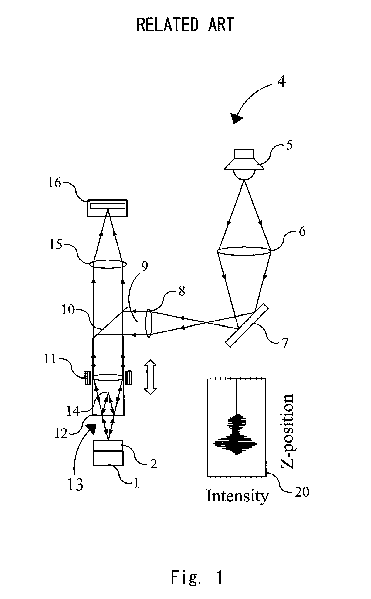
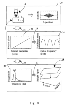
Method and apparatus for performing film thickness measurements using white light scanning interferometry
PatentActiveUS20120218560A1
Innovation
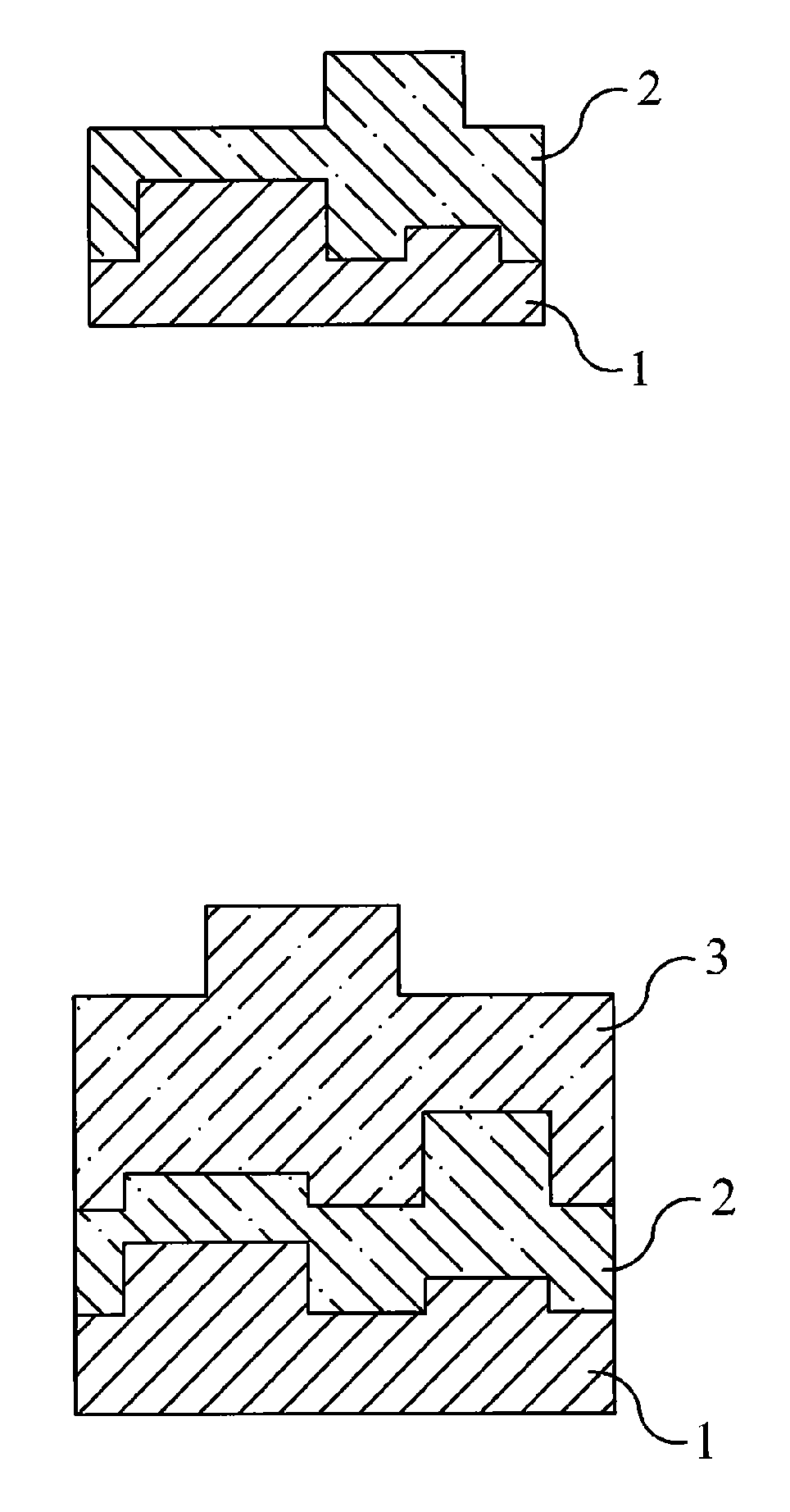
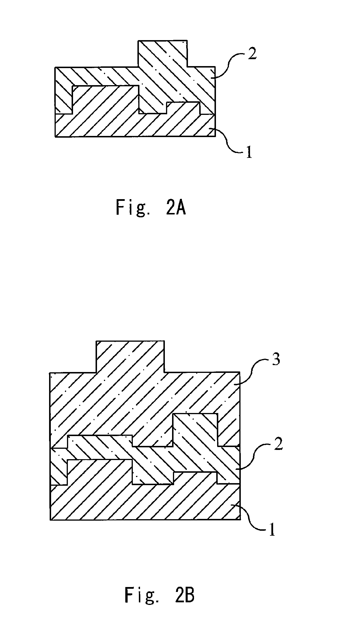
- The method involves removing the linear component of the Fourier phase function to obtain a non-linear component, applying a second integral transformation to obtain an integral amplitude function, identifying the peak location, and determining the film thickness as twice the abscissa at the peak location, considering the refractive index dependent on wavelength, thereby eliminating the need for optimization and enhancing measurement speed.
Materials Science Considerations and Limitations
The optimization of film thickness and strain for performance gains is fundamentally constrained by several materials science principles that must be carefully considered. Crystalline structure integrity represents a primary limitation, as exceeding critical thickness thresholds inevitably leads to strain relaxation through defect formation. These defects—primarily dislocations and stacking faults—significantly degrade electrical and optical properties, creating an upper boundary for effective strain engineering.
Lattice mismatch between substrate and film materials introduces inherent limitations to the degree of strain that can be maintained in epitaxial systems. While pseudomorphic growth enables coherent interfaces up to critical thickness, the accumulated elastic energy eventually forces relaxation through various mechanisms. This fundamental trade-off between thickness and maintainable strain creates a design constraint that cannot be circumvented through conventional approaches.
Thermal stability considerations further complicate optimization efforts, as strain states often exhibit temperature-dependent behavior. High-temperature processing steps can trigger premature relaxation or unwanted interdiffusion at interfaces, potentially negating carefully engineered strain profiles. Materials with disparate thermal expansion coefficients may experience additional strain evolution during thermal cycling, introducing reliability concerns for device operation.
Interface quality emerges as another critical limitation, with atomic-level roughness and chemical intermixing significantly influencing strain transfer efficiency. Perfect interfaces are theoretical constructs rarely achieved in practice, with real systems exhibiting various non-idealities that reduce effective strain coupling. Advanced characterization techniques reveal that interfacial regions often possess unique properties distinct from both substrate and film, creating additional complexity.
Material selection itself imposes constraints on achievable performance gains. While certain semiconductor combinations theoretically offer substantial strain-induced band structure modifications, practical considerations such as lattice parameter compatibility, thermal stability, and process integration often limit material choices to a narrower subset than theoretically optimal.
Metastability of highly strained films presents long-term reliability challenges, as thermodynamically unfavorable strain states may gradually relax during device operation. This time-dependent behavior necessitates accelerated testing protocols to predict performance degradation pathways and establish realistic lifetime expectations for strained film technologies.
Economic Feasibility and Scaling Potential
The economic feasibility of optimizing film thickness and strain for performance gains depends significantly on the balance between implementation costs and resulting benefits. Initial capital investments for advanced deposition equipment capable of precise thickness control and strain engineering can range from $500,000 to several million dollars, representing a substantial barrier to entry for smaller manufacturers. However, these costs must be evaluated against potential long-term savings and revenue increases.
Material efficiency improvements present a compelling economic case. Optimized thin films can reduce raw material consumption by 15-30% compared to conventional approaches, particularly significant for expensive materials like noble metals or rare earth elements. This translates to direct cost savings that can help offset initial equipment investments within 2-3 years of implementation.
Energy consumption considerations also factor prominently in economic assessments. Thinner films generally require less energy during deposition processes, with studies indicating potential energy savings of 10-25% depending on the specific materials and techniques employed. These operational savings compound over time, improving the overall return on investment.
Scaling potential varies considerably across different application domains. In semiconductor manufacturing, the economic benefits of optimized film thickness and strain are most readily realized due to established high-volume production infrastructure and the critical importance of performance gains. The cost-per-wafer reduction can reach 5-12% when considering both material savings and yield improvements.
For emerging applications like flexible electronics and photovoltaics, scaling challenges remain more pronounced. Current production methods often struggle to maintain precise thickness and strain control across large areas, limiting immediate economic benefits. However, roll-to-roll processing technologies show promise for overcoming these limitations, potentially reducing production costs by up to 40% compared to batch processing methods.
Market adoption timelines differ significantly based on industry maturity. Established semiconductor manufacturers can typically implement optimized film technologies within 1-2 years, while emerging sectors may require 3-5 years before widespread adoption becomes economically viable. This adoption curve directly impacts return on investment calculations and should inform strategic implementation planning.
Risk assessment must also consider potential yield impacts during technology transition periods. Initial implementation typically experiences a 3-8% yield reduction before process optimization, temporarily offsetting economic benefits. Manufacturers must account for this transition period in their financial planning to ensure sustainable implementation.
Unlock deeper insights with Patsnap Eureka Quick Research — get a full tech report to explore trends and direct your research. Try now!
Generate Your Research Report Instantly with AI Agent
Supercharge your innovation with Patsnap Eureka AI Agent Platform!