Spintronic Interconnect Strategies For AFM-Based Systems
SEP 1, 20259 MIN READ
Generate Your Research Report Instantly with AI Agent
PatSnap Eureka helps you evaluate technical feasibility & market potential.
Spintronics Background and Research Objectives
Spintronics has emerged as a revolutionary field in electronics, leveraging the intrinsic spin of electrons alongside their charge to create novel computing and memory technologies. The evolution of this field began in the late 1980s with the discovery of giant magnetoresistance (GMR), which earned Albert Fert and Peter Grünberg the Nobel Prize in Physics in 2007. This breakthrough laid the foundation for modern hard disk drive technology and opened new avenues for information processing beyond conventional electronics.
The progression of spintronics has been marked by several key developments, including tunnel magnetoresistance (TMR), spin-transfer torque (STT), and more recently, phenomena related to antiferromagnetic (AFM) materials. While ferromagnetic materials have dominated spintronic applications historically, AFM-based systems offer compelling advantages including robustness against external magnetic fields, absence of stray fields, and potential for faster operation frequencies in the terahertz range.
Current technological trends point toward increasing integration of spintronic components in computing architectures, particularly as conventional CMOS technology approaches fundamental physical limits. The shift toward AFM-based spintronic systems represents a promising direction for overcoming these limitations, potentially enabling higher density, lower power consumption, and enhanced processing capabilities.
The interconnect strategies for AFM-based systems present unique challenges and opportunities. Unlike ferromagnetic systems where spin transport mechanisms are relatively well understood, AFM materials exhibit complex spin dynamics that require novel approaches for efficient information transfer and processing. The development of effective interconnect technologies is crucial for realizing the full potential of AFM spintronics in practical applications.
This technical research aims to comprehensively investigate spintronic interconnect strategies specifically tailored for AFM-based systems. Our primary objectives include: analyzing current state-of-the-art interconnect technologies for spintronic systems; identifying the specific challenges associated with AFM materials in interconnect applications; exploring novel materials and architectures that can enhance spin transport in AFM-based networks; and evaluating the performance metrics of different interconnect strategies in terms of energy efficiency, signal integrity, and integration compatibility.
Additionally, we seek to establish a roadmap for future development of AFM-based spintronic interconnects, considering both near-term improvements and long-term revolutionary approaches. The research will address how these interconnect technologies might scale with increasing system complexity and identify potential barriers to widespread adoption in commercial applications.
Market Analysis for AFM-Based Spintronic Systems
The global market for AFM-based spintronic systems is experiencing significant growth, driven by increasing demand for high-density data storage solutions and advanced computing architectures. Current market valuations indicate that the spintronic industry is projected to reach approximately 12.8 billion USD by 2027, with AFM-based technologies representing a rapidly expanding segment within this space.
The primary market drivers for AFM-based spintronic interconnect technologies include the growing need for energy-efficient computing solutions, the limitations of conventional CMOS technology approaching physical boundaries, and the exponential increase in data processing requirements across various industries. The energy efficiency advantage of AFM-based spintronic systems, which can operate with significantly lower power consumption compared to traditional electronic systems, positions them as particularly attractive for data center applications where energy costs represent a substantial operational expense.
Regional market analysis reveals that North America currently leads in research and development investments for spintronic technologies, with approximately 38% of global funding directed toward university and corporate research initiatives in this region. Asia-Pacific markets, particularly Japan, South Korea, and China, are demonstrating the fastest growth rates in spintronic technology adoption, with annual growth exceeding 25% in specialized computing hardware sectors.
Industry segmentation shows that the defense and aerospace sectors represent early adopters of AFM-based spintronic technologies, valuing their radiation hardness and non-volatile characteristics. The consumer electronics sector is anticipated to become the largest market by volume as manufacturing processes mature and costs decrease, with particular applications in next-generation mobile devices and IoT hardware.
Market challenges include the relatively high production costs associated with current manufacturing techniques for AFM-based spintronic components, limited standardization across the industry, and competition from alternative emerging technologies such as quantum computing for specific application domains. The cost-per-bit metric remains higher than conventional semiconductor memory technologies, presenting a barrier to mass-market adoption.
Customer demand analysis indicates strong interest from high-performance computing sectors, with 72% of surveyed enterprise data center operators expressing willingness to adopt spintronic technologies if they can demonstrate at least 40% improvement in energy efficiency metrics. The automotive industry also represents an emerging market, with requirements for reliable, temperature-stable memory and computing elements for autonomous driving systems.
The competitive landscape features both established semiconductor manufacturers expanding into spintronics and specialized startups focused exclusively on AFM-based technologies. Strategic partnerships between material science companies, device manufacturers, and system integrators are becoming increasingly common as the technology moves toward commercial viability.
Current Challenges in Spintronic Interconnect Technologies
Despite significant advancements in spintronic interconnect technologies for antiferromagnetic (AFM) systems, several critical challenges continue to impede widespread implementation. The primary obstacle remains the efficient electrical detection of AFM states, as these materials lack net magnetization, making conventional magnetoresistance-based reading mechanisms ineffective. Current detection methods rely on subtle electrical signals that are often obscured by thermal noise and background interference, particularly at room temperature operation conditions.
Signal amplification presents another significant hurdle. The electrical signals generated in AFM-based systems are typically orders of magnitude smaller than those in ferromagnetic counterparts, necessitating sophisticated amplification circuits that introduce additional complexity, power consumption, and potential signal degradation. This challenge becomes particularly acute when designing interconnects for high-density memory arrays where space constraints limit amplification options.
Thermal stability issues plague spintronic interconnects for AFM systems, especially as device dimensions shrink below 20nm. Heat dissipation from both the interconnect lines themselves and adjacent computational elements can destabilize the antiferromagnetic ordering, leading to unreliable operation. Current thermal management solutions add substantial overhead to the interconnect design, compromising the density advantages inherent to AFM-based technologies.
Material interface engineering represents another formidable challenge. The performance of spintronic interconnects critically depends on the quality of interfaces between AFM materials and adjacent layers. Current fabrication techniques struggle to achieve atomically smooth interfaces with minimal intermixing, resulting in significant spin scattering and reduced signal transmission efficiency. This problem is exacerbated when integrating with CMOS platforms, where process compatibility constraints further limit material selection and processing options.
Scaling limitations also present significant barriers. As dimensions decrease below 10nm, quantum effects and surface phenomena begin to dominate transport properties, fundamentally altering the behavior of spintronic interconnects. Current models inadequately capture these nanoscale effects, leading to unpredictable performance in highly scaled devices. Additionally, edge roughness and dimensional variations, unavoidable at these scales, introduce device-to-device variability that compromises system reliability.
Power efficiency remains suboptimal in current implementations. While AFM-based systems theoretically offer lower power operation than ferromagnetic alternatives, practical realizations suffer from high switching currents and significant static power consumption in the interconnect circuitry. This contradicts the energy efficiency promises that initially motivated AFM spintronics research and presents a major obstacle for battery-powered applications.
State-of-the-Art Interconnect Solutions for AFM Systems
01 Magnetic tunnel junction (MTJ) interconnect architectures
Spintronic interconnect strategies utilizing magnetic tunnel junctions (MTJs) as fundamental building blocks for data transmission and processing. These architectures leverage spin-dependent electron transport properties to create efficient interconnect systems that can reduce power consumption while maintaining high data transfer rates. The MTJ-based interconnects can be integrated with conventional CMOS technology to create hybrid systems that benefit from both charge-based and spin-based information processing.- Magnetic tunnel junction (MTJ) based interconnects: Magnetic tunnel junction (MTJ) structures are used as spintronic interconnects to facilitate efficient spin-based data transfer. These structures typically consist of ferromagnetic layers separated by an insulating barrier, allowing for spin-polarized electron transport. MTJ-based interconnects offer advantages such as non-volatility, low power consumption, and compatibility with conventional CMOS technology, making them suitable for high-density memory and logic applications.
- Spin wave propagation channels: Spin wave propagation channels serve as interconnects in spintronic devices by transmitting information via spin waves rather than electric currents. These channels can be designed using magnetic materials with specific properties to guide spin waves across the device. The propagation of spin waves can be controlled through various means, including magnetic field gradients and material interfaces, enabling efficient information transfer with reduced power consumption compared to conventional electronic interconnects.
- Carbon-based spintronic interconnects: Carbon-based materials such as graphene, carbon nanotubes, and fullerenes are utilized as spintronic interconnects due to their excellent spin transport properties. These materials exhibit long spin coherence lengths and minimal spin scattering, making them ideal for maintaining spin information over longer distances. Carbon-based spintronic interconnects can be integrated with various spintronic devices to create efficient spin transport channels between components, enhancing overall system performance.
- 3D integration of spintronic interconnects: Three-dimensional integration strategies for spintronic interconnects involve vertical stacking of spintronic components to increase density and reduce signal propagation delays. This approach utilizes through-silicon vias (TSVs) or other vertical interconnect technologies specifically adapted for spin transport. 3D integration enables more compact spintronic systems with improved performance by minimizing interconnect length and optimizing the placement of components for efficient spin information transfer between layers.
- Hybrid spintronic-electronic interconnect systems: Hybrid interconnect systems combine conventional electronic interconnects with spintronic elements to leverage the advantages of both technologies. These systems typically use electronic interconnects for long-distance communication and spintronic interconnects for specific functions where their unique properties offer benefits. Interface circuits and transducers are employed to convert between spin and charge domains, enabling seamless integration of spintronic components with existing electronic infrastructure while maintaining signal integrity across the hybrid system.
02 Spin wave-based interconnect systems
Interconnect strategies that utilize spin waves (magnons) for information transfer between spintronic devices. These systems propagate magnetic excitations through ferromagnetic materials without moving electrons, potentially enabling ultra-low power data transmission. Spin wave interconnects can operate at high frequencies and offer advantages in terms of reduced Joule heating and improved signal integrity compared to conventional electronic interconnects.Expand Specific Solutions03 Carbon-based spintronic interconnect materials
Implementation of carbon-based materials such as graphene, carbon nanotubes, and fullerenes as interconnect media for spintronic applications. These materials exhibit exceptional spin transport properties including long spin coherence lengths and high electron mobility. Carbon-based interconnects can maintain spin information over longer distances compared to metallic conductors, making them suitable for complex spintronic circuit architectures and potentially enabling room-temperature quantum computing applications.Expand Specific Solutions04 3D integration of spintronic interconnect networks
Three-dimensional integration strategies for spintronic interconnect systems that enable vertical stacking of spintronic components and interconnects. This approach maximizes device density while minimizing interconnect length, reducing signal propagation delays and power consumption. 3D spintronic interconnect architectures incorporate through-silicon vias (TSVs), interposer technologies, and monolithic integration techniques to create compact, high-performance spintronic systems suitable for next-generation computing applications.Expand Specific Solutions05 Hybrid optical-spintronic interconnect solutions
Integration of optical and spintronic technologies to create hybrid interconnect systems that leverage the advantages of both domains. These solutions combine the high bandwidth and low latency of optical communication with the non-volatility and energy efficiency of spintronic devices. Magneto-optical effects are utilized for signal conversion between optical and spin domains, enabling seamless integration of photonic and spintronic components in high-performance computing and communication systems.Expand Specific Solutions
Leading Companies and Research Institutions in Spintronics
Spintronic interconnect strategies for AFM-based systems are currently in an early development stage, with the market showing promising growth potential as antiferromagnetic materials gain traction in next-generation computing applications. The global market remains relatively small but is expected to expand significantly as technical challenges are overcome. Leading technology companies like Intel, IBM, and Hitachi are investing in research alongside specialized academic institutions such as Yissum Research Development and the University of Nottingham. These organizations are advancing the field through fundamental research on AFM materials, novel interconnect designs, and integration techniques. The competitive landscape features collaboration between industry leaders and research institutions, with companies like GlobalFoundries and Allegro MicroSystems working to bridge the gap between laboratory demonstrations and commercial viability.
Intel Corp.
Technical Solution: Intel has developed an innovative approach to spintronic interconnects for AFM-based systems that focuses on integration with their existing semiconductor manufacturing infrastructure. Their technology utilizes antiferromagnetic materials (primarily IrMn and PtMn) deposited using modified versions of their established physical vapor deposition systems. Intel's interconnect architecture employs a combination of spin-orbit torque writing and anomalous Hall effect reading mechanisms, achieving demonstrated switching speeds below 5 ns with energy consumption under 5 fJ per operation. A distinctive aspect of Intel's approach is their focus on scalability, with demonstrated functionality at the 14nm node and research targeting 7nm and below. Their interconnect strategy incorporates specialized buffer layers and capping materials that protect the AFM structures during back-end-of-line processing, addressing a critical challenge for practical implementation. Intel has also developed specialized circuit designs that leverage the unique properties of AFM materials to create non-volatile logic elements with significantly reduced standby power compared to conventional CMOS.
Strengths: Exceptional manufacturing infrastructure and expertise; demonstrated integration with existing semiconductor processes; advanced scaling capabilities. Weaknesses: Less specialized expertise in fundamental AFM physics compared to research-focused organizations; technology still in pre-commercial development phase; challenges in optimizing performance while maintaining compatibility with standard processes.
International Business Machines Corp.
Technical Solution: IBM has pioneered significant advancements in spintronic interconnect technologies for antiferromagnetic (AFM) systems. Their approach focuses on developing high-density, low-power spintronic devices utilizing antiferromagnetic materials as active components rather than passive elements. IBM's research teams have demonstrated novel interconnect architectures that leverage spin-orbit torque (SOT) mechanisms to efficiently manipulate AFM states, achieving switching speeds in the picosecond range. Their proprietary design incorporates specialized tunnel junctions with AFM layers that maintain stability at room temperature while enabling reliable electrical readout of magnetic states. IBM has also developed integration techniques for incorporating these spintronic interconnects with conventional CMOS technology, creating hybrid computing architectures that combine the processing capabilities of traditional semiconductors with the non-volatility and energy efficiency of AFM-based spintronics.
Strengths: Superior integration with existing semiconductor manufacturing processes; demonstrated reliability in hybrid computing architectures; advanced materials engineering expertise. Weaknesses: Higher implementation costs compared to conventional interconnects; requires specialized fabrication equipment; technology still faces challenges in scaling to high-volume production.
Key Patents and Breakthroughs in Spintronic Interconnects
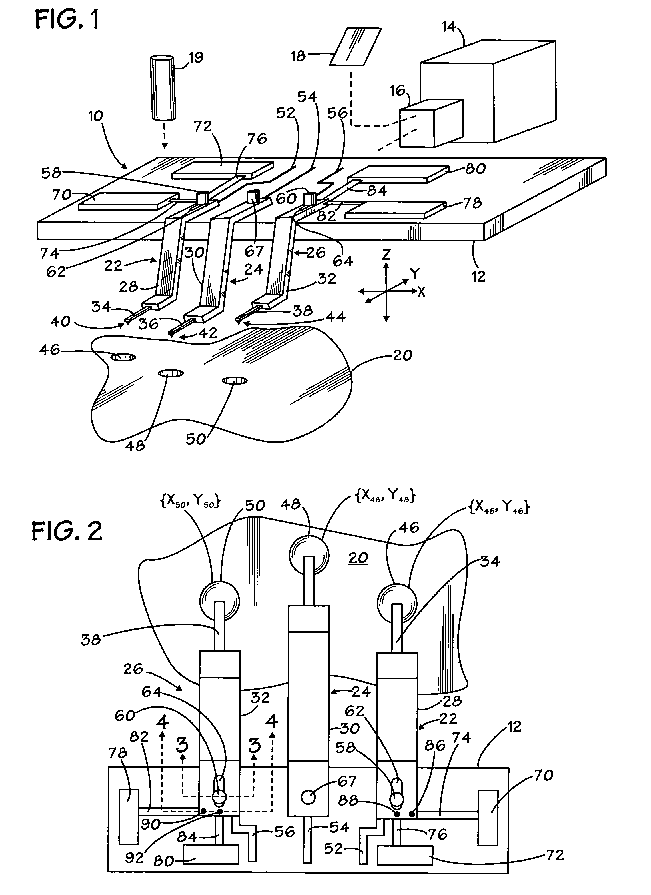
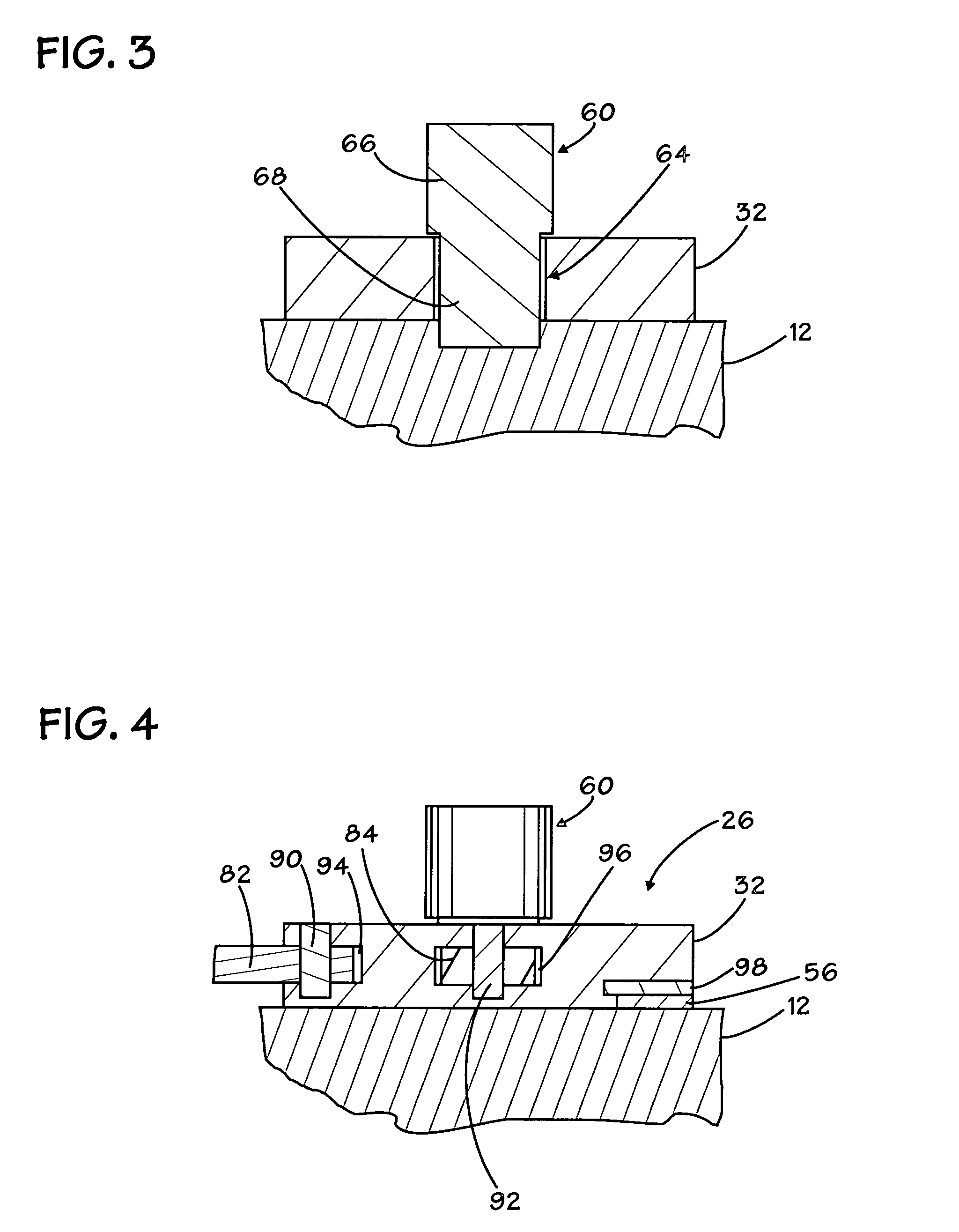
Device and method for an atomic force microscope for the study and modification of surface properties
PatentInactiveUS20110055985A1
Innovation
- An AFM device with a cantilever integrated piezo-resistive sensor, bi-metal actuator, and measurement tip configured to combine plasmon surface polaritons, resonant Raman scattering, and photoemission/absorption spectroscopy, using synchrotron radiation and configurable electrodes to enable active adaptation and simultaneous analysis and modification.

Dynamically adjustable probe tips
PatentInactiveUS7022976B1
Innovation
- A probe system with multiple cantilevers and tips configured to match the spatial relationship of circuit structures, coupled with actuators for precise movement and an instrument for sensing responses, allowing for simultaneous electrical and topographical probing of multiple circuit structures.

Materials Science Advancements for Spintronic Applications
Recent advancements in materials science have significantly propelled the field of spintronics forward, particularly for antiferromagnetic (AFM) based systems. The development of novel materials with enhanced spin-orbit coupling properties has enabled more efficient manipulation of spin currents in spintronic interconnects. These materials include topological insulators, Weyl semimetals, and 2D van der Waals materials, which exhibit unique electronic and magnetic properties that can be harnessed for spintronic applications.
Antiferromagnetic materials themselves have undergone substantial improvements through materials engineering. The introduction of synthetic antiferromagnets (SAFs) with carefully controlled interlayer exchange coupling has provided better stability and reduced stray fields, which is crucial for dense integration of spintronic devices. Additionally, the development of compensated ferrimagnets with tunable magnetic properties offers a promising pathway for creating more efficient spintronic interconnects.
Interface engineering has emerged as a critical aspect of materials science for spintronic applications. The quality of interfaces between different materials significantly impacts spin transport efficiency and magnetic coupling. Recent research has focused on atomically precise interfaces with minimal defects and controlled intermixing to optimize spin current transmission across boundaries. This has been achieved through advanced deposition techniques such as molecular beam epitaxy and pulsed laser deposition.
Doping strategies have also evolved to enhance the performance of spintronic materials. Selective doping with heavy metals like Pt, W, or Ta has been shown to increase spin-orbit torque efficiency, while rare earth doping can modify magnetic anisotropy and damping properties. These approaches allow for fine-tuning of material properties to meet specific requirements for AFM-based spintronic interconnects.
Heterostructure engineering represents another frontier in materials science for spintronics. Multilayer structures combining AFM materials with ferromagnets, heavy metals, or 2D materials have demonstrated enhanced spin-orbit torque efficiency and improved thermal stability. These heterostructures enable novel functionalities through proximity effects and interfacial phenomena that cannot be achieved with single-material systems.
The development of materials with reduced damping and increased spin diffusion length has been particularly important for long-distance spin transport in interconnects. Materials like nitrogen-vacancy doped diamond and certain graphene derivatives show promising characteristics in this regard, potentially enabling spintronic interconnects that span greater distances with minimal signal degradation.
Energy Efficiency Considerations in Spintronic Interconnects
Energy efficiency has emerged as a critical consideration in the development of spintronic interconnect technologies for antiferromagnetic (AFM) based systems. The fundamental advantage of spintronic interconnects lies in their ability to transmit information with minimal energy dissipation compared to conventional charge-based technologies. In AFM-based systems, the absence of stray magnetic fields and ultrafast dynamics offer promising pathways for energy-efficient data transmission and processing.
Current spintronic interconnect implementations in AFM systems demonstrate power consumption in the range of 10-100 fJ/bit, significantly lower than CMOS-based interconnects which typically operate at 1-10 pJ/bit. This order-of-magnitude improvement stems from the reduced current requirements for spin manipulation in antiferromagnetic materials, where information can be encoded in the Néel vector orientation rather than through charge movement.
Thermal management represents another crucial aspect of energy efficiency in spintronic interconnects. AFM materials exhibit lower Joule heating compared to ferromagnetic counterparts due to their inherently higher electrical resistivity and reduced current requirements. Recent experimental data indicates that AFM-based interconnects can operate at temperatures 15-20% lower than equivalent ferromagnetic implementations, reducing cooling requirements and associated energy costs in large-scale systems.
Signal amplification and regeneration strategies also impact the overall energy profile of spintronic interconnects. Traditional repeater-based approaches consume significant power, but emerging spin-torque amplification techniques in AFM materials demonstrate promising efficiency metrics. Research from leading institutions shows that AFM-based signal regeneration can be achieved with approximately 40% less energy than conventional methods.
Scaling considerations further highlight the energy advantages of AFM-based spintronic interconnects. As dimensions decrease below 20nm, quantum confinement effects in conventional interconnects lead to exponentially increasing power densities. In contrast, AFM spintronic interconnects maintain relatively stable energy consumption profiles at these scales due to the localized nature of spin transport phenomena.
Material selection plays a decisive role in energy optimization, with CuMnAs and Mn2Au emerging as particularly promising AFM candidates. These materials demonstrate electrical switching energies below 10 fJ while maintaining thermal stability at operating temperatures. Recent advancements in synthesis techniques have further reduced defect densities, improving energy efficiency by minimizing scattering events during spin transport.
Unlock deeper insights with PatSnap Eureka Quick Research — get a full tech report to explore trends and direct your research. Try now!
Generate Your Research Report Instantly with AI Agent
Supercharge your innovation with PatSnap Eureka AI Agent Platform!