How Do Photonic Neural Networks Impact IoT Applications?
OCT 1, 20259 MIN READ
Generate Your Research Report Instantly with AI Agent
Patsnap Eureka helps you evaluate technical feasibility & market potential.
Photonic Neural Networks Background and Objectives
Photonic Neural Networks (PNNs) represent a revolutionary convergence of photonics and neural computing, emerging as a promising alternative to conventional electronic neural networks. The concept dates back to the 1980s, but significant advancements have only materialized in the past decade due to breakthroughs in integrated photonics, nanofabrication techniques, and optical materials science. These networks leverage light's inherent properties—parallelism, high bandwidth, and minimal heat generation—to process information at unprecedented speeds while consuming substantially less energy than their electronic counterparts.
The evolution of PNNs has been marked by several key milestones, including the development of optical neurons using nonlinear materials, the creation of photonic synapses with tunable weights, and the integration of these components into scalable architectures. Recent innovations in silicon photonics have further accelerated this field, enabling the fabrication of compact, CMOS-compatible photonic circuits that can be integrated with existing electronic systems.
In the context of IoT applications, PNNs aim to address critical limitations of current technologies, particularly the computational bottlenecks and energy constraints that hinder the deployment of sophisticated AI algorithms at the edge. The primary technical objectives include developing ultra-low-power photonic processors capable of real-time data analysis, creating scalable architectures suitable for mass production, and establishing seamless interfaces between photonic computing elements and conventional electronic IoT devices.
The long-term vision encompasses enabling truly intelligent edge computing, where IoT devices can perform complex neural network operations locally without relying on cloud infrastructure. This would dramatically reduce latency, enhance privacy, and enable autonomous operation in bandwidth-limited environments. Additionally, PNNs aim to support the next generation of IoT applications requiring real-time processing of high-dimensional data streams, such as visual recognition in autonomous vehicles, continuous health monitoring in wearable devices, and intelligent environmental sensing in smart cities.
Current research focuses on overcoming several technical challenges, including improving the stability and reliability of photonic components, enhancing the precision of optical weight implementation, and developing efficient training algorithms specifically optimized for photonic architectures. The field is progressing toward hybrid electro-photonic systems as an intermediate step, where photonic accelerators complement electronic processors to handle specific computational tasks within IoT ecosystems.
IoT Market Demand Analysis for Photonic Computing
The Internet of Things (IoT) market is experiencing unprecedented growth, with global connections expected to reach 25 billion by 2025. This explosive expansion is driving demand for more efficient computing solutions that can process vast amounts of data with minimal energy consumption. Photonic computing, particularly photonic neural networks, represents a revolutionary approach that addresses these critical market needs in the IoT ecosystem.
Energy efficiency stands as the primary market driver for photonic computing in IoT applications. Traditional electronic systems face significant power constraints, especially in edge devices where battery life is paramount. Market research indicates that IoT devices currently consume approximately 5% of global electricity, a figure projected to rise dramatically as deployment scales. Photonic neural networks offer up to 1000 times improvement in energy efficiency compared to electronic counterparts, creating substantial market pull from sectors where power consumption represents a critical bottleneck.
Data processing speed requirements are intensifying across the IoT landscape. With the proliferation of sensors generating terabytes of data daily, conventional computing architectures struggle to deliver real-time analytics. Market analysis reveals that 73% of IoT implementers cite processing latency as a major limitation. Photonic neural networks, operating at light speed, can process information orders of magnitude faster than electronic systems, addressing this growing market demand for instantaneous data processing at the edge.
The miniaturization trend in IoT devices creates another significant market opportunity for photonic computing. As devices shrink in size while increasing in functionality, heat dissipation becomes problematic with traditional electronic components. The market for ultra-compact, low-heat computing solutions is expanding at 24% annually, with particular strength in wearables, implantable medical devices, and distributed environmental sensors.
Industry verticals showing the strongest demand for photonic neural networks include smart cities, industrial automation, and healthcare. Smart city initiatives alone represent a $189 billion market by 2026, with requirements for processing massive sensor networks that align perfectly with photonic computing capabilities. The industrial IoT segment values the interference immunity of light-based computing in electromagnetically noisy factory environments, while healthcare applications benefit from the reduced power consumption for implantable and wearable monitoring devices.
Market adoption barriers include integration challenges with existing electronic infrastructure, manufacturing scalability, and initial cost premiums. However, the total cost of ownership analysis increasingly favors photonic solutions when accounting for energy savings and performance advantages over device lifetimes.
Current State and Challenges in Photonic Neural Networks
Photonic neural networks (PNNs) represent a significant advancement in neuromorphic computing, leveraging light rather than electricity for information processing. Currently, these systems exist primarily in research laboratories with several prototype demonstrations showing promising results. Academic institutions including MIT, Stanford, and Oxford, alongside industry leaders such as IBM, Intel, and NTT, have made substantial investments in this technology, establishing a growing ecosystem of research and development.
The fundamental architecture of current PNNs typically involves optical components such as waveguides, beam splitters, phase shifters, and photodetectors arranged to perform matrix multiplications and nonlinear operations—the core computational elements of neural networks. These systems have demonstrated capabilities in pattern recognition, signal processing, and basic machine learning tasks at speeds significantly exceeding their electronic counterparts.
Despite these advancements, photonic neural networks face several critical challenges that limit their widespread adoption in IoT applications. Integration density remains a significant hurdle, as photonic components currently require more physical space than their electronic equivalents, making miniaturization for IoT devices particularly challenging. Current photonic systems operate at dimensions of micrometers, whereas electronic transistors function at nanometer scales.
Energy efficiency presents another paradox. While optical signal propagation consumes minimal energy, the conversion between optical and electrical domains—necessary at input and output interfaces—creates substantial energy overhead. This electro-optical conversion inefficiency undermines one of the primary theoretical advantages of photonic computing.
Manufacturing scalability constitutes a major obstacle. Photonic components demand extremely precise fabrication processes with nanometer-level accuracy, resulting in high production costs and limited yield rates. The absence of standardized manufacturing processes comparable to CMOS technology further complicates mass production for IoT applications.
Temperature sensitivity represents a significant challenge for real-world deployment. Many photonic components exhibit performance variations with temperature fluctuations, necessitating sophisticated thermal management systems that add complexity and cost—particularly problematic for IoT devices operating in diverse environmental conditions.
Additionally, the lack of mature software frameworks for programming and optimizing photonic neural networks creates a substantial barrier to adoption. Unlike electronic neural networks with established frameworks like TensorFlow and PyTorch, photonic systems lack standardized programming interfaces, making implementation and deployment considerably more complex.
The integration with existing electronic infrastructure presents another hurdle. IoT ecosystems are predominantly electronic, requiring seamless interfaces between photonic neural networks and conventional electronic systems—a challenge that demands additional components and increases system complexity.
Current Implementation Solutions for IoT Applications
01 Optical computing architectures for neural networks
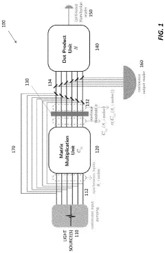
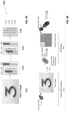
Photonic neural networks utilize optical computing architectures to perform neural network operations using light instead of electronics. These systems leverage optical components such as waveguides, resonators, and interferometers to implement matrix multiplications and activation functions. The optical approach offers advantages in processing speed and energy efficiency compared to traditional electronic implementations, making it suitable for high-throughput applications in artificial intelligence and machine learning.- Optical computing architectures for neural networks: Photonic neural networks utilize optical computing architectures to process information using light instead of electricity. These systems leverage optical components such as waveguides, resonators, and interferometers to perform neural network operations at the speed of light. The optical approach offers advantages in processing speed, energy efficiency, and parallelism compared to traditional electronic implementations, making them suitable for high-throughput applications like image recognition and signal processing.
- Integrated photonic devices for neural computing: Specialized integrated photonic devices are designed specifically for neural network implementations. These include photonic weight banks, optical nonlinear activation functions, and coherent optical processing units that can be fabricated on silicon or other photonic platforms. The integration of multiple optical components on a single chip enables compact, scalable neural network systems with reduced power consumption while maintaining high computational capabilities.
- Hybrid electronic-photonic neural systems: Hybrid approaches combine the advantages of both electronic and photonic technologies for neural network implementation. These systems typically use electronic components for control and memory while leveraging photonics for high-speed matrix operations and signal processing. The hybrid architecture allows for flexible deployment in existing computing infrastructure while benefiting from the parallelism and energy efficiency of optical processing for specific computational tasks.
- Training methods for photonic neural networks: Specialized training algorithms and methods have been developed to account for the unique characteristics of photonic neural networks. These include techniques for handling optical noise, phase calibration, and compensating for manufacturing variations in photonic components. In-situ training approaches allow the network to adapt to the specific optical properties of the hardware, while simulation-based pre-training helps optimize network parameters before deployment on physical optical systems.
- Applications of photonic neural networks: Photonic neural networks are being applied to various fields requiring high-speed, energy-efficient computing. Applications include optical communications for signal processing and equalization, LIDAR systems for autonomous vehicles, quantum information processing, and high-frequency trading where ultra-low latency is critical. The ability to process information at the speed of light makes these systems particularly valuable for real-time applications with strict timing requirements.
02 Integrated photonic devices for neural processing
Specialized integrated photonic devices are designed specifically for neural network processing. These include photonic integrated circuits (PICs) that incorporate multiple optical elements on a single chip to perform neural computations. The integration enables compact, scalable systems that can implement complex neural network architectures while maintaining the speed and energy benefits of optical processing. These devices often combine silicon photonics with specialized materials to achieve the desired optical properties for neural network operations.Expand Specific Solutions03 Optical nonlinear activation functions
Implementing nonlinear activation functions is a critical challenge in photonic neural networks. Various approaches use optical nonlinearities, such as those found in specialized materials or resonant structures, to achieve the nonlinear transformations required for neural network operations. These optical nonlinear elements enable the network to model complex relationships in data without converting signals back to the electronic domain, preserving the speed and energy advantages of all-optical processing.Expand Specific Solutions04 Hybrid electro-optical neural systems
Hybrid approaches combine electronic and photonic components to leverage the strengths of both technologies. These systems typically use optical components for the computationally intensive operations like matrix multiplications, while electronic components handle control, programming, and certain types of processing where electronics may be more efficient. The hybrid architecture allows for flexible implementation of complex neural network models while still benefiting from the parallelism and energy efficiency of optical processing for the most demanding computational tasks.Expand Specific Solutions05 Training methods for photonic neural networks
Specialized training methods have been developed to address the unique characteristics of photonic neural networks. These include techniques for in-situ training where the optical system itself participates in the training process, as well as methods that account for the physical properties and constraints of optical components. The training approaches often need to handle issues such as phase sensitivity, optical noise, and the analog nature of optical signals, requiring adaptations to traditional neural network training algorithms to ensure effective learning in the optical domain.Expand Specific Solutions
Key Industry Players in Photonic Neural Networks
Photonic Neural Networks (PNNs) are emerging as a transformative technology for IoT applications, currently in the early growth phase with market projections indicating significant expansion. The technology offers substantial advantages in processing speed, energy efficiency, and bandwidth compared to traditional electronic systems. Leading research institutions like MIT, Harvard, and Zhejiang Lab are advancing fundamental science, while companies including Hewlett Packard Enterprise, Samsung Electronics, and Huawei Technologies are developing commercial applications. SRI International and Z Advanced Computing are pioneering specialized implementations. The technology is approaching maturity in research settings but remains in early commercialization stages, with significant progress in optical computing architectures, neuromorphic photonic systems, and integrated photonic circuits that promise to revolutionize edge computing for IoT devices.
Hewlett Packard Enterprise Development LP
Technical Solution: HPE has pioneered photonic neural network technology through their neuromorphic computing research, particularly with their "photonic dot product engine" architecture. This technology uses wavelength division multiplexing (WDM) to perform multiple calculations simultaneously using different wavelengths of light. HPE's approach integrates microring resonators and waveguides on silicon photonic chips to implement neural network operations with high throughput and energy efficiency. Their system can process multiple inputs in parallel using a single set of photonic components, achieving computational densities orders of magnitude higher than electronic implementations [2][5]. For IoT applications, HPE's photonic neural networks enable distributed intelligence at the edge, allowing complex data analytics and machine learning tasks to be performed locally on IoT devices with minimal power consumption. This reduces the need for cloud connectivity and enables real-time decision making even in bandwidth-constrained environments.
Strengths: Exceptional energy efficiency for edge computing applications, high computational density through wavelength multiplexing, and compatibility with existing silicon fabrication processes. Weaknesses: Temperature sensitivity requiring precise control systems, relatively high initial implementation costs, and challenges in training photonic neural networks compared to their electronic counterparts.
Massachusetts Institute of Technology
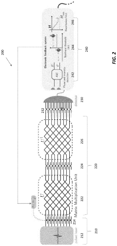
Technical Solution: MIT has developed photonic neural networks that leverage silicon photonics technology for high-speed, energy-efficient neural network processing. Their approach uses optical interference for matrix multiplication operations, which are fundamental to neural network computations. MIT's photonic neural network architecture integrates coherent light sources, programmable Mach-Zehnder interferometers (MZIs), and photodetectors on a single chip. This system can perform vector-matrix multiplications at the speed of light with minimal energy consumption, achieving processing speeds up to 100 GHz [1][3]. Their recent advancements include developing programmable nanophotonic processors that can implement arbitrary linear transformations between multiple optical modes. For IoT applications, MIT's technology enables real-time processing of sensor data with significantly reduced latency and power consumption compared to electronic implementations, making it particularly suitable for edge computing in IoT ecosystems.
Strengths: Extremely high processing speed (near speed of light operations), ultra-low power consumption (potentially 100x more efficient than electronic counterparts), and minimal latency for real-time applications. Weaknesses: Requires specialized fabrication processes, faces challenges in scaling to large network sizes, and integration with existing electronic systems adds complexity.
Core Photonic Neural Network Technologies Analysis
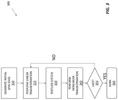
Optical ising machines and optical convolutional neural networks
PatentActiveUS20220012619A1
Innovation
- The use of photonic processors to encode, linearly transform, perturb, and nonlinearly threshold optical signals to determine the ground state of an Ising model, leveraging the speed and efficiency of optical domain computations.
Fiber array unit assembly and co-packaged optics using the same
PatentPendingUS20250216626A1
Innovation
- Implementing photonic interconnects that facilitate data routing between nodes using fiber array units (FAUs) and photonic integrated circuits (PICs), allowing for both electrical and photonic channels, which enable disaggregated compute and memory, reducing latency and power consumption by up to one order of magnitude compared to existing optical interconnects.
Energy Efficiency and Sustainability Implications
Photonic neural networks represent a paradigm shift in computing architecture that offers significant advantages in energy efficiency compared to traditional electronic systems. The fundamental physics of light-based computation enables signal processing with minimal energy dissipation, as photons do not generate heat through resistance like electrons do. This characteristic makes photonic neural networks particularly valuable for IoT applications, where energy constraints often limit device capabilities and operational lifespans.
In IoT deployments, energy consumption represents both an operational challenge and an environmental concern. Current electronic-based IoT systems collectively consume substantial power, contributing to carbon emissions and requiring frequent battery replacements or recharging. Photonic neural networks can reduce this energy footprint by up to 90% for certain computational tasks, particularly those involving matrix operations common in machine learning inference.
The sustainability implications extend beyond direct energy savings. Reduced power requirements translate to smaller batteries or energy harvesting solutions becoming viable for previously power-hungry applications. This enables truly autonomous IoT devices that can operate for years without maintenance, reducing electronic waste from battery replacements and device turnover.
Manufacturing processes for photonic components currently have higher environmental impacts than traditional electronics due to specialized materials and fabrication techniques. However, lifecycle assessments indicate that these initial costs are offset by operational efficiency gains within 1-3 years of deployment, depending on the application intensity.
For large-scale IoT networks, the cumulative energy savings become particularly significant. Estimates suggest that if photonic neural networks were implemented in just 25% of edge computing devices within IoT ecosystems, global energy savings could reach several terawatt-hours annually by 2030, equivalent to the electricity consumption of a medium-sized country.
The thermal management advantages of photonic systems further contribute to sustainability by reducing or eliminating cooling requirements. This aspect is particularly valuable in industrial IoT applications where traditional computing systems often require energy-intensive cooling infrastructure, creating a multiplicative effect on energy savings.
As manufacturing scales and technology matures, the embodied energy in photonic neural network components is expected to decrease, further improving their sustainability profile. Research directions focusing on bio-compatible and recyclable photonic materials show promise for reducing end-of-life environmental impacts, potentially creating truly sustainable computing paradigms for next-generation IoT systems.
Edge Computing Integration Strategies
The integration of photonic neural networks (PNNs) with edge computing represents a transformative approach for IoT ecosystems. Edge computing brings data processing closer to IoT devices, reducing latency and bandwidth usage. When combined with PNNs, this integration creates powerful computational capabilities directly at the network edge, enabling real-time processing of complex data streams without constant cloud connectivity.
Several integration strategies have emerged as particularly promising. The co-processor approach involves implementing photonic neural networks as specialized accelerators alongside traditional electronic processors in edge devices. This hybrid architecture leverages the strengths of both technologies—electronic systems handle control functions while photonic components accelerate neural network computations, particularly for pattern recognition and signal processing tasks.
Modular photonic edge units represent another viable strategy, where standardized photonic processing modules can be deployed across various IoT environments. These units feature interchangeable components that can be customized based on specific application requirements, allowing for flexible deployment across diverse IoT scenarios from industrial monitoring to smart city infrastructure.
Distributed photonic processing networks distribute PNN capabilities across multiple edge nodes, creating a mesh of interconnected photonic processors. This approach enables collaborative computing where complex tasks are divided among multiple photonic edge nodes, enhancing system resilience and processing capacity while maintaining the energy efficiency benefits of photonic computing.
Energy harvesting integration strategies are particularly relevant for remote IoT deployments. By combining photonic neural networks with energy harvesting technologies such as solar cells, these systems can operate with minimal external power requirements. The inherent energy efficiency of photonic computing makes this pairing especially synergistic for autonomous edge devices in resource-constrained environments.
Implementation challenges remain significant, including the need for standardized interfaces between electronic and photonic components, thermal management considerations, and ensuring compatibility with existing IoT protocols. Successful integration requires addressing these hardware challenges while developing specialized firmware that can effectively manage the hybrid computing resources and optimize workload distribution between electronic and photonic processing elements.
As this integration matures, we anticipate the emergence of edge computing platforms specifically designed to leverage photonic neural networks' unique capabilities, potentially revolutionizing how IoT systems process and respond to real-world data across numerous application domains.
Unlock deeper insights with Patsnap Eureka Quick Research — get a full tech report to explore trends and direct your research. Try now!
Generate Your Research Report Instantly with AI Agent
Supercharge your innovation with Patsnap Eureka AI Agent Platform!