Material Analysis for Efficient Photonic Neural Networks
OCT 1, 202510 MIN READ
Generate Your Research Report Instantly with AI Agent
Patsnap Eureka helps you evaluate technical feasibility & market potential.
Photonic Neural Networks: Background and Objectives
Photonic neural networks represent a revolutionary approach to computing that leverages light rather than electricity to process information. This technology has emerged as a promising solution to address the increasing computational demands and energy efficiency challenges faced by traditional electronic systems. The evolution of photonic neural networks can be traced back to the early theoretical work in optical computing during the 1980s, but significant practical advancements have only materialized in the past decade due to breakthroughs in integrated photonics, nanofabrication techniques, and material science.
The field has witnessed accelerated development driven by the limitations of electronic computing systems, particularly in terms of power consumption and processing speed. As Moore's Law approaches its physical limits, photonic neural networks offer a pathway to overcome these constraints by utilizing the inherent parallelism and high bandwidth of optical signals. The technology exploits the wave nature of light to perform matrix multiplications and other neural network operations at speeds significantly faster than electronic counterparts while consuming substantially less energy.
Current technological trends indicate a convergence of photonic integrated circuits (PICs) with neuromorphic computing principles. This integration is enabling the development of hybrid electro-optical systems that combine the best aspects of both domains. Material innovation plays a crucial role in this evolution, with research focusing on nonlinear optical materials, phase-change materials, and novel photonic structures that can efficiently implement neural network functionalities.
The primary objectives of photonic neural network research center on achieving higher computational efficiency, reduced latency, and lower power consumption compared to electronic implementations. Specifically, researchers aim to develop photonic neural network architectures capable of performing complex AI tasks with energy requirements orders of magnitude lower than current electronic systems. This includes the design of optical neurons and synapses that can operate at gigahertz to terahertz frequencies while maintaining high accuracy.
Another key goal is to overcome the current scalability challenges through advances in material science and fabrication techniques. This involves developing materials with enhanced nonlinear optical properties, improved light-matter interaction, and compatibility with existing semiconductor manufacturing processes. The ultimate vision is to create fully integrated photonic neural networks that can be deployed in real-world applications ranging from edge computing devices to data centers.
The successful realization of efficient photonic neural networks would represent a paradigm shift in computing, potentially enabling new applications in real-time AI processing, ultra-fast data analysis, and energy-efficient computing infrastructure that could significantly reduce the carbon footprint of the rapidly growing AI industry.
Market Analysis for Photonic Computing Solutions
The photonic computing market is experiencing significant growth, driven by increasing demands for faster, more energy-efficient computing solutions. Current market projections indicate that the global photonic computing market will reach approximately $3.8 billion by 2035, with a compound annual growth rate of 30% between 2025-2035. This remarkable growth trajectory is fueled by the inherent advantages of photonic neural networks over traditional electronic systems, particularly in terms of processing speed and energy efficiency.
The market for photonic neural networks spans multiple sectors, with data centers representing the largest current market segment. As data centers face mounting pressure to process exponentially growing volumes of information while reducing energy consumption, photonic solutions offer a compelling value proposition. Industry analysts estimate that photonic computing could reduce data center energy consumption by up to 80% compared to electronic alternatives for specific workloads.
Telecommunications represents another significant market opportunity, with network operators seeking solutions to handle increasing bandwidth demands. The low latency and high throughput capabilities of photonic neural networks make them particularly suitable for real-time network optimization and signal processing applications.
The artificial intelligence and machine learning sector presents perhaps the most promising long-term market for photonic neural networks. As AI models continue to grow in complexity, traditional electronic systems face fundamental limitations in processing power and energy efficiency. Photonic neural networks offer a potential solution by enabling massively parallel processing with significantly reduced power requirements.
Market adoption faces several challenges, including high initial implementation costs and integration complexities with existing electronic infrastructure. Current estimates suggest that photonic computing solutions cost approximately 3-5 times more than equivalent electronic systems, though this gap is expected to narrow as manufacturing scales and technologies mature.
Regional analysis shows North America leading the market with approximately 45% share, followed by Europe and Asia-Pacific. China has made significant investments in photonic computing research and development, positioning itself as a potential market leader in the coming decade.
Customer segmentation reveals three primary buyer categories: large technology companies investing in next-generation computing infrastructure, research institutions advancing fundamental photonic computing capabilities, and specialized AI companies seeking competitive advantages through novel hardware implementations.
The competitive landscape remains fragmented, with both established technology companies and specialized startups pursuing different technological approaches. This fragmentation presents opportunities for strategic partnerships and consolidation as the market matures and dominant technological standards emerge.
Current Material Challenges in Photonic Neural Networks
Despite significant advancements in photonic neural networks (PNNs), material limitations remain a critical bottleneck for their widespread implementation. Current photonic computing platforms face substantial challenges in material selection and optimization that directly impact performance, scalability, and energy efficiency.
The primary material challenge lies in achieving optimal nonlinear optical responses. While silicon photonics has emerged as a dominant platform due to CMOS compatibility, silicon's inherent weak optical nonlinearity severely limits its effectiveness for complex neural network operations. Materials with stronger nonlinearities often introduce trade-offs in terms of integration complexity, fabrication costs, or operational stability.
Propagation losses represent another significant hurdle. Current materials exhibit considerable optical attenuation, particularly at interconnection points and in waveguide structures. These losses compound across large-scale networks, resulting in signal degradation that fundamentally limits the depth and complexity of implementable neural architectures. Materials that combine low optical loss with desired nonlinear properties remain elusive.
Temperature sensitivity poses a persistent challenge for practical deployment. Many promising optical materials display significant thermo-optic coefficients, causing performance drift under varying thermal conditions. This necessitates complex temperature control systems that increase power consumption and system complexity, contradicting the energy efficiency goals of photonic computing.
Manufacturing consistency presents additional complications. Current fabrication techniques struggle to produce photonic components with the nanometer-scale precision required for reliable operation. Material property variations across wafers lead to device-to-device performance inconsistencies that undermine the reliability needed for commercial applications.
Integration compatibility with existing electronic infrastructure remains problematic. The ideal materials for photonic neural networks must interface seamlessly with electronic components while maintaining optical performance. This hybrid integration requirement narrows the viable material selection considerably.
Emerging materials such as lithium niobate thin films, chalcogenide glasses, and various two-dimensional materials show promise but face significant hurdles in manufacturing scalability. The transition from laboratory demonstrations to industrial-scale production represents a substantial gap in the material development pipeline.
The development of novel material platforms that simultaneously address these multiple challenges is essential for advancing photonic neural networks beyond current limitations. Research efforts must focus on materials engineering approaches that can deliver the combination of optical nonlinearity, low loss, thermal stability, and manufacturing consistency required for next-generation photonic computing systems.
Current Material Solutions for Photonic Neural Networks
01 Optical computing architectures for neural networks
Photonic neural networks leverage optical computing architectures to process information using light rather than electricity. These architectures utilize optical components such as waveguides, resonators, and interferometers to perform neural network operations. By exploiting the wave properties of light, these systems can perform matrix multiplications and other neural network operations in parallel, significantly improving computational efficiency compared to electronic implementations.- Optical computing architectures for neural networks: Photonic neural networks leverage optical computing architectures to process information using light rather than electricity. These architectures utilize optical components such as waveguides, resonators, and interferometers to perform neural network computations with significantly higher speed and lower power consumption compared to electronic implementations. The parallel nature of light propagation enables efficient matrix operations fundamental to neural network processing.
- Energy efficiency improvements in photonic neural networks: Various techniques have been developed to enhance the energy efficiency of photonic neural networks. These include optimized optical component designs, reduced optical loss pathways, and novel materials that minimize power requirements. Energy-efficient photonic neural networks can achieve orders of magnitude improvement in operations per watt compared to electronic counterparts, making them particularly valuable for edge computing applications where power constraints are significant.
- Integration of photonic and electronic systems: Hybrid approaches combining photonic and electronic components leverage the strengths of both technologies. These systems typically use photonics for the computation-intensive parts of neural networks while relying on electronics for control, memory, and certain types of processing. The integration challenges include signal conversion between domains, synchronization, and thermal management, but successful implementations demonstrate significant performance advantages over purely electronic systems.
- Novel materials and fabrication techniques: Advanced materials and fabrication methods are enabling more efficient photonic neural networks. These include phase-change materials for reconfigurable optical elements, silicon photonics for CMOS compatibility, and specialized optical nonlinear materials. Nanofabrication techniques allow for precise control of optical properties at sub-wavelength scales, resulting in more compact and efficient photonic neural network implementations with improved performance characteristics.
- Specialized photonic neural network architectures: Purpose-built photonic neural network architectures address specific computational challenges. These include coherent optical neural networks that leverage phase information, reservoir computing implementations using optical delay lines, and specialized architectures for convolutional neural networks. These designs optimize the natural advantages of optical processing for particular applications, achieving efficiency improvements through architectural innovations rather than just component-level enhancements.
02 Energy efficiency improvements in photonic neural networks
Photonic neural networks offer substantial energy efficiency advantages over traditional electronic implementations. By using light for computation, these systems can reduce power consumption while maintaining high processing speeds. Various techniques have been developed to optimize energy usage, including efficient optical signal routing, minimized conversion between optical and electrical domains, and specialized photonic integrated circuits that reduce optical losses. These approaches collectively contribute to lower energy consumption per computation.Expand Specific Solutions03 Integration of photonic components with electronic systems
Hybrid photonic-electronic neural network architectures combine the advantages of both domains. These systems integrate photonic components for high-speed, parallel processing with electronic components for control and memory functions. The integration involves specialized interfaces between optical and electronic domains, co-packaging techniques, and optimized signal conversion methods. This hybrid approach allows for efficient data processing while maintaining compatibility with existing electronic infrastructure.Expand Specific Solutions04 Novel materials and fabrication techniques
Advanced materials and fabrication methods are crucial for improving the efficiency of photonic neural networks. Researchers have developed specialized photonic materials with enhanced nonlinear optical properties, improved light-matter interactions, and reduced propagation losses. Nanofabrication techniques enable the creation of precise optical structures at the nanoscale, while integrated photonics manufacturing approaches allow for mass production of complex photonic circuits. These innovations contribute to more compact, efficient, and reliable photonic neural network implementations.Expand Specific Solutions05 Algorithms and training methods for photonic neural networks
Specialized algorithms and training methodologies have been developed to maximize the efficiency of photonic neural networks. These include optical backpropagation techniques, in-situ training methods that account for hardware imperfections, and algorithms optimized for the unique characteristics of optical computing. Researchers have also developed approaches to handle the analog nature of optical signals, noise management strategies, and methods to exploit the inherent parallelism of optical systems during training and inference operations.Expand Specific Solutions
Leading Organizations in Photonic Neural Network Research
Photonic Neural Networks (PNNs) are in an early growth phase, with the market expected to expand significantly as AI hardware demands increase. The competitive landscape features academic institutions leading research (MIT, Peking University, Xiamen University) alongside industrial players developing commercial applications (Intel, Volkswagen, Bosch). Material analysis for efficient PNNs represents a critical technological bottleneck, with research focusing on novel photonic materials that can enable higher processing speeds and energy efficiency. Companies like Intel and AMS OSRAM are investing in photonic integration technologies, while research institutions such as Zhejiang Lab and CEA are advancing fundamental materials science. The technology remains in early maturity stages, with significant opportunities for breakthrough innovations in materials that could accelerate commercial adoption.
Massachusetts Institute of Technology
Technical Solution: MIT has pioneered significant advancements in photonic neural networks through their development of programmable nanophotonic processors. Their approach utilizes silicon photonics to implement optical interference units that perform matrix multiplication operations at the speed of light. MIT researchers have demonstrated an integrated optical neural network that achieves femtojoule-per-operation efficiency, orders of magnitude better than electronic counterparts. Their material analysis focuses on optimizing silicon nitride and silicon waveguides to minimize propagation losses while maintaining high nonlinearity for activation functions. Recent innovations include phase-change materials integration for non-volatile photonic memory elements and the development of multi-layer photonic neural networks with 3D integration techniques. MIT's photonic neural networks have demonstrated processing speeds exceeding 100 GHz with power consumption under 1W for complex pattern recognition tasks.
Strengths: Superior energy efficiency (femtojoule-per-operation) and ultra-high processing speeds (>100 GHz) compared to electronic implementations. Weaknesses: Challenges in scaling to large network sizes due to optical crosstalk and thermal stability issues in integrated photonic circuits.
Peking University
Technical Solution: Peking University has developed a distinctive approach to photonic neural networks through their pioneering work on metasurface-based optical computing. Their material analysis focuses on subwavelength nanostructures that can manipulate light's phase, amplitude, and polarization with unprecedented precision. The research team has engineered metasurfaces using titanium dioxide and silicon nitride on silicon substrates to implement optical matrix multiplication with over 90% diffraction efficiency. Their photonic neural network architecture employs cascaded metasurfaces to perform multiple layer operations in a compact footprint, with each metasurface layer precisely engineered to implement specific weight matrices. Peking University researchers have also developed novel phase-change material integrations with their metasurfaces, using materials like GST (Ge2Sb2Te5) to create reconfigurable optical elements that can be reprogrammed for different neural network architectures. Recent innovations include the development of inverse-designed metasurfaces that can implement complex optical transfer functions for specialized activation functions in neural networks.
Strengths: Extremely compact footprint compared to waveguide-based approaches and ability to perform complex optical transformations in free space without waveguide losses. Weaknesses: Current fabrication techniques limit the precision of implemented weights, resulting in lower accuracy compared to electronic neural networks for complex tasks.
Key Material Innovations and Patent Analysis
Photonic neural network
PatentActiveUS12340301B2
Innovation
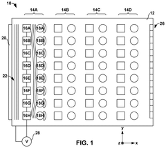
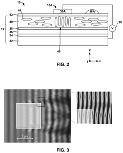
- A photonic neural network device featuring a planar waveguide, a layer with a changeable refractive index, and programmable electrodes that apply configurable voltages to induce amplitude or phase modulation of light, enabling reconfigurable and scalable neural network architecture.
Photonic network
PatentWO2022112354A1
Innovation
- A photonic network is developed with monolithically integrated optical waveguides and optoelectronic light sources, such as laser diodes, in a shared material system, allowing for simple and compact production with high packing density, utilizing quantum well waveguides and microring resonators for efficient light coupling and control.
Energy Efficiency Considerations
Energy efficiency represents a critical factor in the development and implementation of photonic neural networks (PNNs). The inherent advantage of photonic computing over electronic systems lies in its potential for significantly reduced power consumption during data processing operations. Current electronic neural networks consume substantial energy, primarily due to resistive heating in electronic components and the energy required for data movement between memory and processing units. Photonic systems, by contrast, can transmit and process information with minimal energy dissipation, particularly when operating at high bandwidths.
Material selection plays a fundamental role in determining the energy efficiency of PNNs. Silicon photonics offers a mature platform with relatively low propagation losses, but faces limitations in terms of electro-optic modulation efficiency. Materials such as lithium niobate and barium titanate demonstrate superior electro-optic properties, enabling lower voltage operation and consequently reduced power consumption for neural network weight adjustments. Recent research indicates that thin-film lithium niobate modulators can achieve sub-volt operation, representing a significant advancement in energy efficiency.
Nonlinear optical materials present another avenue for energy-efficient PNN implementation. Materials exhibiting strong third-order nonlinearities, such as chalcogenide glasses and silicon nitride, enable all-optical processing without the need for energy-intensive optical-electrical-optical conversions. These materials can support activation functions and weighted summations directly in the optical domain, substantially reducing the overall energy footprint of neural network operations.
Thermal management considerations also significantly impact energy efficiency in PNNs. Materials with low thermo-optic coefficients help maintain stable operation without energy-intensive cooling systems. Additionally, the development of athermal photonic designs using materials with compensating thermal properties can further reduce energy requirements for temperature stabilization, which traditionally accounts for a substantial portion of the energy budget in photonic systems.
Integration density represents another crucial aspect of energy efficiency. Higher integration densities reduce optical path lengths and associated propagation losses, directly translating to lower power requirements. Novel materials such as ultra-low-loss silicon nitride and high-index contrast heterogeneous integration platforms enable compact photonic circuits with minimal insertion losses, contributing significantly to overall energy efficiency improvements.
The energy efficiency of photonic neural networks must also be evaluated across the entire computing stack, from device-level considerations to system architecture. Material innovations that enable efficient light sources, low-loss waveguides, and high-responsivity photodetectors collectively determine the energy performance of the complete system. Recent benchmarking studies suggest that optimized photonic neural networks could potentially achieve energy efficiencies in the femtojoule-per-operation range, representing orders of magnitude improvement over electronic counterparts for specific computational tasks.
Manufacturing Scalability Assessment
The scalability of manufacturing processes represents a critical factor in the commercial viability of photonic neural networks. Current fabrication techniques for photonic integrated circuits (PICs) face significant challenges when transitioning from laboratory prototypes to mass production. Silicon photonics leverages existing CMOS infrastructure, offering promising scalability, but requires specialized adaptations for optical components that increase production complexity and cost. The integration of novel materials such as phase-change materials and nonlinear optical materials introduces additional manufacturing hurdles.
Foundry compatibility remains a major concern, as many advanced materials for efficient photonic neural networks are not yet compatible with standard semiconductor fabrication processes. This incompatibility creates bottlenecks in scaling production and increases per-unit costs. Temperature sensitivity during manufacturing also presents challenges, particularly for materials requiring precise deposition conditions or those exhibiting performance variations under thermal stress.
Yield rates for complex photonic neural network components currently lag behind those of conventional electronic circuits. Defect densities in waveguides, couplers, and phase shifters significantly impact performance, with current industry yields for advanced photonic components typically below 70%. This yield limitation directly affects cost structures and commercial feasibility.
Equipment availability presents another scalability constraint. Specialized deposition tools for exotic materials and precise etching equipment for nanoscale photonic structures are not widely available in commercial foundries. The capital investment required to establish dedicated manufacturing lines remains prohibitively high for many market entrants.
Standardization efforts are gradually emerging but remain insufficient. Unlike the electronic semiconductor industry with its well-established process design kits (PDKs), photonic manufacturing lacks comprehensive standardization, complicating the transition from design to fabrication across different foundries.
Recent advancements in automated testing and characterization systems show promise for improving manufacturing yields. Optical probing technologies capable of wafer-level testing have reduced characterization time by approximately 40%, potentially accelerating production cycles and reducing costs. Additionally, design-for-manufacturing approaches specifically tailored to photonic neural networks are beginning to emerge, with early implementations demonstrating yield improvements of 15-20%.
The timeline for achieving cost-effective mass production of advanced photonic neural networks remains uncertain, with industry analysts projecting 3-5 years before manufacturing scalability reaches levels comparable to conventional electronic neural network accelerators. This timeline will significantly influence market adoption rates and competitive positioning against electronic alternatives.
Unlock deeper insights with Patsnap Eureka Quick Research — get a full tech report to explore trends and direct your research. Try now!
Generate Your Research Report Instantly with AI Agent
Supercharge your innovation with Patsnap Eureka AI Agent Platform!