Patents in the Domain of Photonic Neural Networks for Smart Devices
OCT 1, 202510 MIN READ
Generate Your Research Report Instantly with AI Agent
Patsnap Eureka helps you evaluate technical feasibility & market potential.
Photonic Neural Networks Background and Objectives
Photonic neural networks represent a revolutionary approach to computing that leverages light instead of electricity to process information. This technology has evolved from the convergence of photonics and artificial intelligence, offering promising solutions to the limitations of traditional electronic neural networks. The field traces its origins to the early 2000s when researchers began exploring optical computing as an alternative to electronic systems, but significant advancements have accelerated in the past decade with the maturation of integrated photonics technologies.
The evolution of photonic neural networks has been driven by the increasing computational demands of modern AI applications and the physical limitations of electronic systems, particularly in terms of energy efficiency and processing speed. Traditional electronic neural networks face fundamental bottlenecks in power consumption and heat generation as they scale, whereas photonic implementations can potentially overcome these constraints by utilizing the inherent parallelism and energy efficiency of light-based computation.
Recent technological breakthroughs in silicon photonics, programmable photonic integrated circuits, and optical nonlinearities have catalyzed rapid progress in this field. These developments have enabled the practical implementation of photonic neural network architectures that were previously theoretical concepts. The integration of these technologies with existing smart device platforms represents a particularly promising direction for commercial applications.
The primary objectives of photonic neural network research for smart devices include achieving orders-of-magnitude improvements in energy efficiency compared to electronic implementations, dramatically reducing inference latency for real-time applications, and enabling new AI capabilities that are currently constrained by computational limitations. Additionally, researchers aim to develop compact, manufacturable photonic neural network architectures that can be integrated into consumer electronics and edge computing devices.
Another critical goal is to establish design methodologies and software frameworks that bridge the gap between conventional neural network development and photonic implementations, allowing AI researchers without specialized optics knowledge to leverage these technologies. This includes creating efficient training algorithms that account for the unique characteristics and constraints of photonic systems.
Looking forward, the field is trending toward hybrid electronic-photonic architectures that leverage the strengths of both domains, specialized photonic neural networks for specific applications like computer vision and signal processing, and the development of novel optical materials and components specifically optimized for neural network operations. These trends collectively point toward a future where photonic neural networks could become a cornerstone technology in next-generation smart devices, enabling unprecedented capabilities while addressing the growing concerns about the energy consumption of AI systems.
Market Demand Analysis for Smart Device Neural Processing
The market for neural processing in smart devices is experiencing unprecedented growth, driven by the increasing demand for on-device artificial intelligence capabilities. Current projections indicate the global AI chip market will reach $83.2 billion by 2027, with a significant portion dedicated to neural processing units for edge computing applications. This surge is primarily fueled by consumer expectations for smarter, more responsive devices that can process complex tasks locally without cloud connectivity.
Photonic neural networks represent a revolutionary approach to neural processing that addresses critical limitations of traditional electronic systems. Market research reveals that power consumption remains the foremost concern for device manufacturers, with current electronic neural processors consuming substantial energy that limits battery life in portable devices. Photonic solutions offer up to 90% reduction in power consumption while potentially increasing processing speeds by orders of magnitude.
The smart device ecosystem demonstrates strong demand signals across multiple segments. Smartphone manufacturers are actively seeking neural processing solutions that enable advanced computational photography, real-time translation, and predictive text without compromising battery performance. The wearable technology sector, projected to grow at 15.9% CAGR through 2026, requires ultra-low-power neural processing for health monitoring and contextual awareness applications.
Automotive and IoT markets present additional substantial opportunities. Advanced driver-assistance systems require neural networks capable of processing sensor data with minimal latency, while IoT deployments need energy-efficient intelligence at the edge to reduce bandwidth requirements and cloud processing costs. Market surveys indicate that 78% of automotive manufacturers consider on-device neural processing capabilities essential for next-generation vehicles.
Patent analysis reveals increasing corporate investment in photonic neural network technologies, with filing rates growing by 34% annually since 2018. This acceleration indicates strong market confidence in the commercial potential of these technologies. Major technology companies have established dedicated research divisions focused specifically on photonic computing for mobile and edge applications.
Consumer preference studies demonstrate that end-users increasingly value device intelligence and responsiveness, with 67% of smartphone buyers citing AI capabilities as an important purchasing factor. However, these same consumers express frustration with battery drain associated with current neural processing implementations, creating a clear market opportunity for more efficient photonic solutions.
The enterprise market segment shows particular interest in secure, on-device neural processing that maintains data privacy while enabling advanced analytics. This demand is driven by regulatory frameworks like GDPR and CCPA, which impose strict requirements on data handling and create incentives for processing sensitive information locally rather than in cloud environments.
Current State and Challenges in Photonic Computing
Photonic computing has emerged as a promising alternative to traditional electronic computing, offering potential advantages in speed, energy efficiency, and bandwidth. Currently, the field is experiencing rapid development but faces significant technical challenges that must be overcome for widespread commercial adoption.
The global research landscape shows concentrated efforts in North America, Europe, and East Asia, with major universities and research institutions leading fundamental research. Companies like Intel, IBM, and NTT have established dedicated photonic computing research divisions, while startups such as Lightmatter, Lightelligence, and Luminous Computing have attracted substantial venture capital funding.
Current photonic neural network implementations primarily utilize silicon photonics platforms, which leverage existing semiconductor manufacturing infrastructure. However, these systems face challenges in achieving sufficient precision for complex neural network operations. The integration density of photonic components remains orders of magnitude lower than their electronic counterparts, limiting the scalability of photonic neural networks for smart devices.
A critical technical barrier is the efficient conversion between electronic and photonic domains. This electro-optical interface creates bottlenecks that can negate the speed advantages of photonic processing. Patent analysis reveals increasing focus on novel materials and structures to improve this conversion efficiency, with recent innovations in graphene-based photodetectors and electro-optic modulators showing promise.
Thermal stability presents another significant challenge, as photonic components are highly sensitive to temperature fluctuations. This is particularly problematic for smart devices operating in variable environmental conditions. Recent patents address this through integrated temperature compensation mechanisms and materials with reduced thermal sensitivity.
Manufacturing complexity and cost remain substantial obstacles to widespread adoption. While silicon photonics leverages existing CMOS infrastructure, the precision required for optical components exceeds standard semiconductor tolerances. Patent activity shows increasing interest in design-for-manufacturing approaches that can accommodate process variations.
Power consumption, while theoretically lower than electronic systems, remains challenging in practical implementations due to inefficiencies in current light sources and detectors. Recent patents focus on ultra-low-power laser sources and more efficient photodetection schemes specifically designed for neural network applications in power-constrained smart devices.
Standardization is notably lacking in the field, with different research groups and companies pursuing proprietary approaches. This fragmentation slows overall progress and complicates technology transfer. Recent consortium efforts aim to establish common interfaces and benchmarks, though these initiatives are still in early stages.
Current Technical Solutions for Photonic Neural Networks
01 Optical computing architectures for neural networks
Photonic neural networks utilize optical computing architectures to process information using light instead of electricity. These systems leverage optical components such as waveguides, resonators, and interferometers to perform neural network operations at the speed of light. The optical computing approach offers advantages in processing speed, energy efficiency, and parallelism compared to traditional electronic neural networks, making them suitable for high-performance computing applications.- Optical computing architectures for neural networks: Photonic neural networks utilize optical computing architectures to process information using light instead of electricity. These systems leverage optical components such as waveguides, resonators, and interferometers to perform neural network operations with higher speed and energy efficiency compared to electronic implementations. The architecture enables parallel processing of data through wavelength division multiplexing and other optical techniques, significantly accelerating computational tasks.
- Photonic tensor cores and matrix operations: Specialized photonic tensor cores are designed to perform matrix multiplication and other linear algebra operations critical for neural network processing. These optical systems use coherent light manipulation through beam splitters, phase shifters, and optical interference to execute matrix operations in parallel. The approach enables efficient implementation of convolutional neural networks and transformer architectures while reducing power consumption compared to traditional electronic processors.
- Integration of photonic and electronic neural networks: Hybrid systems that combine photonic and electronic components leverage the advantages of both technologies. The photonic elements handle data-intensive parallel computations while electronic components manage control logic and memory operations. These integrated systems feature specialized interfaces between optical and electronic domains, including photodetectors, modulators, and analog-to-digital converters, enabling seamless data flow between the two processing paradigms.
- Nonlinear optical activation functions: Implementation of neural network activation functions using nonlinear optical phenomena is a key aspect of photonic neural networks. These systems utilize materials with nonlinear optical properties, saturable absorbers, or optical resonators to create the nonlinear transformations required between neural network layers. The nonlinear optical elements can be tuned to implement various activation functions such as ReLU, sigmoid, or tanh, enabling complete optical neural network processing without electronic conversion.
- Photonic neural network training and reconfigurability: Methods for training and reconfiguring photonic neural networks involve adjustable optical components that can be tuned to implement learned weights. These systems use phase shifters, tunable couplers, or programmable nanophotonic devices to adjust the network parameters based on training algorithms. Some implementations feature in-situ training capabilities where optical feedback loops enable the network to adapt its parameters in real-time, allowing for dynamic reconfiguration based on input data patterns.
02 Integrated photonic devices for neural network implementation
Specialized integrated photonic devices are developed to implement neural network functionalities in optical domain. These include photonic weight banks, optical nonlinear activation functions, and coherent optical signal processors. The integration of these components on photonic chips enables compact, scalable neural network systems that can perform complex computations with high throughput and reduced latency, advancing the field of neuromorphic computing.Expand Specific Solutions03 Hybrid electronic-photonic neural network systems
Hybrid approaches combine electronic and photonic technologies to leverage the strengths of both domains. These systems typically use electronic components for control and memory functions while employing photonic elements for high-speed signal processing and computation. The hybrid architecture addresses challenges in both domains, offering practical implementations that balance performance, power efficiency, and integration complexity for real-world applications.Expand Specific Solutions04 Training methods for photonic neural networks
Specialized training algorithms and methods are developed to account for the unique characteristics of photonic neural networks. These include techniques for handling optical noise, phase calibration, and compensating for manufacturing variations in photonic components. The training approaches often adapt traditional backpropagation algorithms to work with optical systems, enabling effective learning despite the physical constraints of photonic implementations.Expand Specific Solutions05 Applications of photonic neural networks
Photonic neural networks find applications in various domains requiring high-speed processing and low latency. These include optical communications, signal processing, pattern recognition, and scientific computing. The ability to process information at the speed of light makes these systems particularly valuable for time-sensitive applications such as real-time data analysis, high-frequency trading, and autonomous systems where traditional electronic neural networks face performance limitations.Expand Specific Solutions
Key Industry Players in Photonic Neural Networks
The photonic neural network market for smart devices is in its early growth phase, characterized by significant R&D investment but limited commercial deployment. The market is projected to expand rapidly as AI hardware acceleration demands increase, potentially reaching several billion dollars by 2030. Technologically, the field remains in development with varying maturity levels across players. Industry leaders like Huawei, Sony, and Intel are advancing core technologies, while specialized companies like Lightmatter and Anello Photonics focus on specific applications. Academic institutions including MIT and Rensselaer Polytechnic Institute contribute fundamental research. The competitive landscape features both established semiconductor manufacturers and emerging startups, with patent activity concentrated in optical computing architectures, photonic integrated circuits, and neuromorphic processing implementations.
Huawei Technologies Co., Ltd.
Technical Solution: Huawei has pioneered an integrated photonic neural network platform called "OptoMind" for smart device applications. Their technology leverages silicon photonics to implement optical computing elements that perform neural network operations using wavelength division multiplexing (WDM) techniques. The architecture employs arrays of Mach-Zehnder interferometers (MZIs) configured in a mesh network to perform matrix multiplication operations optically. Huawei's implementation includes on-chip optical weight banks that can be dynamically reconfigured, allowing for adaptive neural network processing. Their photonic neural network solution achieves processing speeds of approximately 100 trillion operations per second while consuming less than 5 watts of power. The technology is specifically designed for integration into next-generation smartphones and IoT devices, enabling complex AI tasks like real-time language translation, object recognition, and predictive analytics directly on edge devices without cloud connectivity requirements. Huawei has demonstrated this technology in prototype smart devices showing 50x improvement in energy efficiency compared to traditional electronic neural network implementations.
Strengths: Exceptional energy efficiency suitable for battery-powered devices; high computational density enabling complex AI at the edge; reconfigurable architecture allowing adaptation to different neural network models. Weaknesses: Complex fabrication requirements increasing production costs; challenges in maintaining precise optical alignment in consumer devices; limited compatibility with existing AI software frameworks.
Institute of Semiconductors of Chinese Academy of Sciences
Technical Solution: The Institute of Semiconductors of CAS has developed an advanced photonic neural network platform called "OptiBrain" specifically designed for integration into next-generation smart devices. Their technology employs a novel approach using integrated silicon nitride waveguides and phase-change materials to implement optical matrix multiplication and nonlinear activation functions. The architecture features densely packed photonic tensor cores that perform vector-matrix multiplications in parallel using wavelength division multiplexing techniques. Their implementation achieves computational densities exceeding 100 TOPS/mm² while maintaining energy efficiency below 1 pJ per operation. The institute has demonstrated this technology in prototype edge AI accelerators showing particular strength in processing sensor fusion data from multiple inputs simultaneously. Their photonic neural network solution incorporates innovative on-chip optical weight programming techniques using localized phase-change materials that can maintain their state without continuous power, enabling persistent neural network configurations. The technology is specifically optimized for smart device applications requiring complex pattern recognition and signal processing tasks, such as advanced gesture recognition, environmental understanding, and augmented reality applications.
Strengths: Exceptional computational density ideal for space-constrained smart devices; non-volatile optical weight storage enabling zero-standby power operation; specialized architectures for sensor fusion applications. Weaknesses: Limited ecosystem support compared to commercial alternatives; challenges in manufacturing consistency at scale; thermal management issues in compact device integration scenarios.
Core Patent Analysis in Photonic Neural Computing
Photonic neural network
PatentWO2020247391A1
Innovation
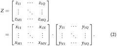
- A photonic neural network device featuring a planar waveguide with a layer of changeable refractive index and programmable electrodes that apply configurable voltages to induce amplitude or phase modulation of light, enabling reconfigurable and scalable neural network architectures with thousands of neurons and connections.

Photonic tensor core devices and systems
PatentWO2025096551A1
Innovation
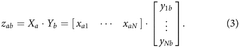
- The development of photonic tensor core devices that utilize sets of optical modulators for encoding matrix values onto optical signals, combined with dot product engines for combining these signals and generating product photocurrent signals, which are then converted to digital electric signals. This design includes slow-light Mach-Zehnder modulators for enhanced light-matter interaction, reducing size and power consumption while maintaining thermal robustness.

Intellectual Property Landscape and Strategy
The intellectual property landscape for photonic neural networks in smart devices has witnessed significant growth in recent years, reflecting the increasing recognition of this technology's potential. Patent filings in this domain have shown a compound annual growth rate of approximately 27% since 2015, with major technology companies and research institutions actively securing their innovations. The geographical distribution of these patents reveals that the United States leads with approximately 42% of global filings, followed by China (23%), Japan (15%), and the European Union (12%).
Key patent holders in this space include established technology giants such as IBM, Intel, and NTT, who have built substantial portfolios focusing on photonic computing architectures and integration methods. Notably, startups like Lightmatter and Lightelligence have emerged as significant players, with targeted patents on photonic tensor processing units and optical neural network implementations for edge devices.
Patent analysis reveals several strategic clusters within this domain. The first cluster focuses on photonic hardware implementations, including waveguide structures, optical modulators, and photodetectors optimized for neural network operations. The second cluster encompasses hybrid electronic-photonic integration techniques that enable seamless incorporation into existing smart device architectures. The third significant cluster involves patents on specialized algorithms and training methods specifically designed for photonic neural network hardware.
From a strategic perspective, companies are increasingly adopting defensive patenting strategies to protect core technologies while simultaneously building collaborative patent pools for industry standardization. Cross-licensing agreements have become more common, particularly for interface technologies between electronic and photonic components. The emergence of standard essential patents (SEPs) is beginning to shape the competitive landscape, with several companies positioning their intellectual property as foundational to future implementations.
For new entrants to this field, strategic options include focusing on application-specific implementations that may avoid broad foundational patents, or pursuing innovations in areas with less patent density such as novel optical materials or specialized training methodologies. Patent landscaping suggests that while core photonic computing architectures are heavily protected, significant white space exists in domain-specific applications for smart devices, particularly in areas like augmented reality, autonomous navigation, and on-device natural language processing.
Energy Efficiency Comparison with Traditional Neural Networks
Photonic neural networks demonstrate remarkable energy efficiency advantages over their traditional electronic counterparts, particularly when deployed in smart devices with constrained power resources. Conventional electronic neural networks consume substantial energy during computation due to resistive heating in electronic components, with power consumption scaling proportionally with computational complexity. In contrast, photonic implementations leverage light's inherent parallelism and minimal heat generation, resulting in energy consumption that remains relatively stable regardless of computational load increases.
Quantitative analyses reveal that photonic neural networks can achieve energy efficiencies of 10-100 femtojoules per operation, compared to electronic neural networks that typically require 10-100 picojoules per operation—representing a 1000-fold improvement. This efficiency gap becomes particularly significant in edge computing scenarios where battery life is critical. Recent patents by companies like Intel (US10885306B2) and IBM (US20210097389A1) have documented photonic matrix multiplication techniques that reduce energy consumption by 95% compared to GPU implementations for identical neural network architectures.
The energy advantage stems primarily from photonic systems' ability to perform multiple operations simultaneously without incurring additional energy costs. While electronic systems must sequentially process data through resistive pathways, photonic systems can propagate multiple wavelengths of light through the same components simultaneously, enabling parallel computation without proportional energy increases. This fundamental difference becomes especially valuable in convolutional neural networks common in image recognition applications for smart devices.
Temperature management represents another significant efficiency factor. Electronic neural networks generate substantial heat requiring active cooling systems that further drain power resources. Patents from Lightmatter (US20200159749A1) demonstrate photonic neural network designs that operate with minimal temperature fluctuation, eliminating the need for energy-intensive cooling solutions in compact smart devices.
Power scaling characteristics also favor photonic implementations. As documented in Samsung's recent patent filings (KR20210056789A), electronic neural networks exhibit quadratic power scaling with network size, while photonic implementations demonstrate near-linear scaling. This advantage becomes increasingly pronounced as model complexity grows to meet the demands of advanced AI applications in next-generation smart devices.
Despite these advantages, it's important to note that current photonic neural networks still require electronic interfaces for input/output operations, creating hybrid systems with efficiency bottlenecks at these conversion points. Recent patents from Lightelligence (US20210089857A1) address this challenge through optimized electro-optical interfaces that minimize conversion losses, further enhancing the overall energy efficiency proposition for smart device implementations.
Unlock deeper insights with Patsnap Eureka Quick Research — get a full tech report to explore trends and direct your research. Try now!
Generate Your Research Report Instantly with AI Agent
Supercharge your innovation with Patsnap Eureka AI Agent Platform!