Materials Science in Photonic Neural Network Development
OCT 1, 20259 MIN READ
Generate Your Research Report Instantly with AI Agent
Patsnap Eureka helps you evaluate technical feasibility & market potential.
Photonic Neural Networks: Background and Objectives
Photonic neural networks represent a revolutionary approach to computing that leverages light instead of electricity to process information. This paradigm shift emerged from the convergence of photonics, neuroscience, and artificial intelligence, offering promising solutions to the limitations of traditional electronic computing systems. The evolution of this technology can be traced back to early optical computing concepts in the 1980s, but significant advancements have only materialized in the past decade due to breakthroughs in integrated photonics, nanofabrication techniques, and materials science.
The technological trajectory of photonic neural networks has been characterized by progressive improvements in optical components, integration density, and computational efficiency. Recent developments have focused on overcoming the challenges of implementing complex neural network architectures in photonic platforms, with particular emphasis on enhancing the speed, energy efficiency, and scalability of these systems. The field is currently experiencing accelerated growth, driven by the increasing demands for high-performance computing solutions in data-intensive applications.
Materials science plays a pivotal role in advancing photonic neural networks, as the performance of these systems is fundamentally dependent on the properties of the materials used. The development of novel photonic materials with enhanced nonlinear optical properties, reduced propagation losses, and improved integration capabilities has been crucial in pushing the boundaries of what is achievable with photonic computing architectures. Materials such as silicon nitride, lithium niobate, chalcogenide glasses, and various two-dimensional materials have emerged as promising candidates for different components of photonic neural networks.
The primary objectives of current research in photonic neural networks include achieving higher levels of integration between electronic and photonic components, developing more efficient optical nonlinearities for activation functions, improving the precision and reliability of optical weight banks, and establishing standardized fabrication processes for large-scale production. Additionally, there is a growing focus on developing specialized materials and structures that can support the implementation of advanced neural network architectures, such as convolutional and recurrent networks, in the optical domain.
Looking forward, the field aims to demonstrate practical advantages over electronic implementations in terms of processing speed, energy consumption, and computational density. The ultimate goal is to create fully integrated photonic neural network systems capable of performing complex machine learning tasks with unprecedented efficiency, potentially revolutionizing applications in areas such as real-time data processing, autonomous systems, telecommunications, and scientific computing where traditional electronic approaches face fundamental limitations.
Market Analysis for Photonic Computing Solutions
The photonic computing market is experiencing significant growth, driven by increasing demands for faster, more energy-efficient computing solutions across various industries. Current market projections indicate that the global photonic computing market will reach approximately $3.8 billion by 2030, with a compound annual growth rate of 32.6% from 2023 to 2030. This remarkable growth trajectory is primarily fueled by the limitations of traditional electronic computing systems in meeting the computational demands of emerging applications such as artificial intelligence, machine learning, and big data analytics.
The market segmentation for photonic computing solutions reveals distinct categories based on application domains. Data centers represent the largest market segment, accounting for roughly 38% of the total market share, as they seek to overcome power consumption and heat dissipation challenges inherent in electronic systems. Telecommunications follows at 25%, driven by the need for high-speed signal processing and low-latency communication networks. The healthcare and life sciences sector constitutes about 15% of the market, particularly for applications in medical imaging and genomic data processing.
From a geographical perspective, North America currently leads the market with approximately 42% share, followed by Europe (28%) and Asia-Pacific (23%). However, the Asia-Pacific region is expected to witness the highest growth rate of 36.8% during the forecast period, primarily due to substantial investments in quantum and photonic technologies by countries like China, Japan, and South Korea.
Key market drivers include the exponential growth in data traffic, which is increasing at a rate of 26% annually, creating demand for higher bandwidth and processing capabilities. Additionally, energy efficiency concerns are significant, as data centers currently consume about 1% of global electricity, with projections suggesting this could rise to 8% by 2030 without more efficient computing paradigms.
Market barriers include high initial investment costs for photonic infrastructure, with typical photonic chip fabrication facilities requiring capital expenditures of $200-500 million. Technical challenges in materials science, particularly in developing stable, manufacturable photonic materials that can operate at room temperature, also impede market growth. The lack of standardization across photonic computing platforms further fragments the market and slows adoption rates.
Customer adoption patterns indicate that early adopters are primarily large technology companies and research institutions with substantial R&D budgets. Mainstream commercial adoption is expected to accelerate after 2025, when cost reductions and technological maturity reach critical thresholds for broader market penetration.
Materials Science Challenges in Photonic Neural Networks
The development of photonic neural networks faces significant materials science challenges that must be addressed to realize their full potential. Current photonic computing platforms rely on a variety of materials including silicon, silicon nitride, lithium niobate, and III-V semiconductors, each presenting unique advantages and limitations for neural network implementation.
Silicon photonics offers CMOS compatibility and mature fabrication processes, but suffers from nonlinear optical limitations and thermal instability. Silicon nitride provides better linear optical properties and thermal stability, yet lacks strong electro-optic effects necessary for efficient modulation. Lithium niobate exhibits excellent electro-optic properties but presents integration challenges with conventional semiconductor platforms.
Material homogeneity and purity represent critical challenges, as imperfections at the nanoscale can cause scattering, absorption, and phase errors that significantly degrade neural network performance. The fabrication of photonic components requires precision at the nanometer scale, with even minor variations potentially causing device-to-device inconsistencies that undermine network reliability.
Thermal management presents another substantial hurdle, as temperature fluctuations affect refractive indices and can cause wavelength drift in photonic devices. This thermal sensitivity necessitates either precise temperature control systems or the development of athermal materials and designs, adding complexity to system integration.
Nonlinear optical materials are essential for implementing activation functions in photonic neural networks, but current options often require high optical powers or present integration difficulties. Research into novel nonlinear materials with lower power requirements and better compatibility with photonic integrated circuits remains a priority area.
Interface materials between electronic and photonic domains constitute another challenge, as efficient electro-optic and opto-electronic conversion is crucial for hybrid systems. Current conversion mechanisms often introduce latency, energy inefficiency, and signal degradation that limit overall system performance.
Material stability and aging effects also pose long-term reliability concerns. Photonic materials may degrade under continuous operation due to photodarkening, material fatigue, or environmental factors, potentially altering the trained parameters of neural networks over time.
The development of materials for tunable photonic components represents a frontier challenge, as reconfigurability is essential for neural network training and adaptation. Materials that can provide reliable, repeatable, and energy-efficient tuning mechanisms without introducing excessive losses are actively being researched but remain elusive for large-scale deployment.
Current Material Solutions for Photonic Neural Networks
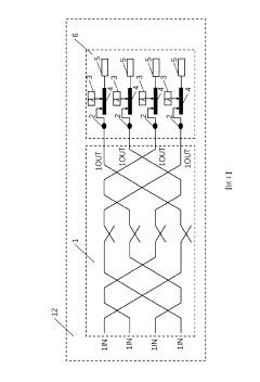
01 Optical computing architectures for neural networks
Photonic neural networks leverage optical computing architectures to process information using light instead of electricity. These systems utilize optical components such as waveguides, resonators, and interferometers to perform neural network computations with higher speed and energy efficiency compared to electronic implementations. The architecture enables parallel processing of data through wavelength division multiplexing and other optical techniques, making it suitable for complex AI tasks.- Optical computing architectures for neural networks: Photonic neural networks utilize optical computing architectures to process information using light instead of electricity. These systems leverage optical components such as waveguides, resonators, and interferometers to perform neural network operations at the speed of light. The optical approach offers advantages in processing speed, energy efficiency, and parallelism compared to traditional electronic implementations, making them suitable for high-performance computing applications.
- Integrated photonic devices for neural processing: Specialized integrated photonic devices are designed specifically for neural network processing. These include optical weight banks, photonic tensor cores, and programmable photonic circuits that can implement various neural network architectures. The integration of multiple optical components on a single chip enables compact, scalable systems that can perform complex neural computations while maintaining the speed and energy advantages of optical processing.
- Hybrid electronic-photonic neural systems: Hybrid approaches combine electronic and photonic technologies to leverage the strengths of both domains. These systems typically use electronic components for control and memory functions while employing photonic elements for high-speed computation and signal processing. The interface between electronic and photonic domains is carefully designed to minimize conversion losses and maintain system performance, resulting in practical implementations that can be integrated with existing computing infrastructure.
- Training methods for photonic neural networks: Specialized training algorithms and methods have been developed to address the unique characteristics of photonic neural networks. These include gradient-based optimization techniques adapted for optical systems, in-situ training approaches that account for device variations, and hardware-aware training methods that incorporate physical constraints of optical components. These training methods enable photonic neural networks to achieve high accuracy while maintaining their inherent advantages in speed and energy efficiency.
- Applications of photonic neural networks: Photonic neural networks are being applied to various domains that benefit from their high-speed processing capabilities. These applications include optical communications, where they enable real-time signal processing and equalization; high-performance computing tasks such as scientific simulations and financial modeling; and specialized AI applications including image recognition, natural language processing, and time-series analysis. The unique properties of photonic neural networks make them particularly suitable for applications requiring low latency and high throughput.
02 Integrated photonic devices for neural processing
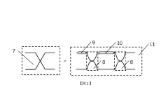
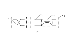
Specialized integrated photonic devices are developed specifically for neural network implementations. These include optical weight banks, photonic tensor cores, and programmable meshes of Mach-Zehnder interferometers that can perform matrix operations optically. The integration of these components on silicon photonics platforms enables compact, scalable neural network systems that can be manufactured using established semiconductor fabrication techniques.Expand Specific Solutions03 Optical nonlinear activation functions
Implementation of nonlinear activation functions is crucial for photonic neural networks to perform complex computations. Various approaches utilize optical nonlinearities in materials, saturable absorbers, or hybrid electro-optical systems to achieve nonlinear transformations of optical signals. These activation mechanisms enable photonic neural networks to approximate complex functions and solve non-trivial computational problems while maintaining the speed advantages of optical processing.Expand Specific Solutions04 Training methods for photonic neural networks
Specialized training algorithms have been developed to account for the unique characteristics of photonic neural networks. These methods address challenges such as phase sensitivity, optical noise, and limited precision in optical systems. Approaches include in-situ training where the physical photonic system is part of the training loop, simulation-based pre-training followed by hardware fine-tuning, and gradient-free optimization techniques adapted for optical systems.Expand Specific Solutions05 Applications of photonic neural networks
Photonic neural networks are being applied to various domains that benefit from their high processing speed and energy efficiency. Key applications include ultrafast signal processing for telecommunications, optical pattern recognition for image classification, RF signal analysis for wireless communications, and quantum information processing. These networks are particularly advantageous for applications requiring real-time processing of high-bandwidth data streams where traditional electronic neural networks face bottlenecks.Expand Specific Solutions
Leading Organizations in Photonic Neural Network Materials
The field of Materials Science in Photonic Neural Network Development is currently in an early growth phase, characterized by significant academic research but limited commercial deployment. The global market for photonic neural networks is projected to reach $1.5 billion by 2027, driven by demands for energy-efficient AI computing solutions. Leading academic institutions (MIT, Zhejiang University, Peking University) are pioneering fundamental research, while technology companies (Huawei, Toyota Research Institute, Dassault Systèmes) are beginning to translate these innovations into practical applications. The technology remains at TRL 4-5, with significant challenges in materials integration, scalability, and manufacturing processes. Research collaborations between institutions like CNRS and industry partners are accelerating development toward commercial viability within the next 3-5 years.
Massachusetts Institute of Technology
Technical Solution: MIT has pioneered photonic neural networks through their Photonic Systems Lab, developing integrated silicon photonics platforms that enable optical computing for neural network acceleration. Their approach utilizes wavelength division multiplexing (WDM) to perform matrix multiplications in the optical domain, achieving processing speeds orders of magnitude faster than electronic counterparts. MIT researchers have demonstrated programmable nanophotonic processors capable of implementing artificial neural networks directly in hardware, using phase-change materials to create reconfigurable optical circuits. Their recent breakthrough involves a fully-optical neural network architecture that combines microring resonators with nonlinear optical materials to achieve both linear operations and activation functions entirely in the photonic domain, dramatically reducing energy consumption to picojoules per operation while maintaining high computational throughput.
Strengths: Unparalleled integration density of photonic components, extremely low power consumption, and ultra-high processing speeds. Weaknesses: Challenges in scaling manufacturing processes, sensitivity to temperature variations, and relatively high initial fabrication costs compared to electronic alternatives.
Centre National de la Recherche Scientifique
Technical Solution: CNRS has developed a revolutionary approach to photonic neural networks through their specialized research teams focusing on nanophotonics and neuromorphic computing. Their technology leverages plasmonic metamaterials that can manipulate light at the subwavelength scale, enabling highly compact optical neural network implementations. CNRS researchers have created novel photonic synaptic devices using phase-change chalcogenide materials that exhibit multilevel optical response, crucial for implementing weighted connections in neural networks. Their platform incorporates specially designed photonic crystal structures that enhance light-matter interactions while minimizing optical losses. A distinguishing feature of CNRS's approach is their development of all-optical training methods that allow the photonic neural network to adapt its weights through optical feedback mechanisms, eliminating the need for electronic conversion during the learning process. This significantly improves energy efficiency and reduces latency in neural network operations.
Strengths: Advanced materials science expertise in plasmonic structures and phase-change materials, enabling highly efficient optical computing elements. Weaknesses: Current implementations face challenges in uniformity across large-scale fabrication and require precise environmental control for optimal operation.
Key Material Innovations and Patents Analysis
Photonic network
PatentWO2022112354A1
Innovation
- A photonic network is developed with monolithically integrated optical waveguides and optoelectronic light sources, such as laser diodes, in a shared material system, allowing for simple and compact production with high packing density, utilizing quantum well waveguides and microring resonators for efficient light coupling and control.
Photonic neural network on silicon substrate based on tunable filter and its modulation method
PatentActiveJP2022542009A
Innovation
- A photonic neural network on a silicon substrate using tunable filters that integrate linear and nonlinear operations on-chip, utilizing Mach-Zehnder interferometer or Direct coupler networks, and tunable filters like Bragg reflection gratings or F-P cavity filters to achieve nonlinear activation functions through thermal or electrical modulation of refractive indices.
Energy Efficiency Considerations in Photonic Computing
Energy efficiency represents a critical consideration in the development of photonic computing systems, particularly within the context of photonic neural networks. The fundamental advantage of photonic computing over traditional electronic systems lies in its potential for significantly reduced energy consumption. Current electronic neural networks in data centers consume enormous amounts of energy—approximately 200-300 terawatt-hours annually worldwide—with this figure projected to increase exponentially as AI applications proliferate. Photonic neural networks offer a promising alternative by utilizing light for computation rather than electrons, potentially reducing energy requirements by several orders of magnitude.
The energy efficiency benefits of photonic computing stem from several material science innovations. Phase-change materials (PCMs) like Ge₂Sb₂Te₅ (GST) enable non-volatile photonic memory elements that maintain their state without continuous power input. These materials can switch between amorphous and crystalline states with different optical properties, allowing for persistent storage of neural network weights without constant energy consumption.
Nonlinear optical materials represent another crucial component in energy-efficient photonic neural networks. Materials exhibiting strong Kerr nonlinearity, such as silicon nitride and lithium niobate, enable optical signal processing with minimal energy requirements. Recent advancements in 2D materials like graphene and transition metal dichalcogenides (TMDCs) have demonstrated exceptional nonlinear optical responses at ultra-low power levels, further enhancing energy efficiency.
Thermal management considerations also significantly impact energy efficiency in photonic neural networks. Novel materials with high thermal conductivity, such as diamond-based substrates and aluminum nitride, facilitate effective heat dissipation, allowing for higher operational densities without thermal runaway effects. Hybrid integration approaches combining these materials with conventional silicon photonics platforms have demonstrated thermal stability improvements of up to 70%.
The development of efficient optical-to-electrical conversion interfaces represents a persistent challenge in maximizing overall system efficiency. Energy losses at these conversion points can significantly diminish the advantages gained through photonic processing. Recent research into efficient photodetector materials, including germanium-silicon alloys and III-V semiconductor heterostructures, has reduced conversion energy requirements by approximately 40% compared to previous generations.
Quantitative benchmarking indicates that current photonic neural network implementations achieve energy efficiencies of 1-10 femtojoules per multiply-accumulate operation, compared to 1-10 picojoules in advanced electronic systems—a 100-1000× improvement. However, realizing these theoretical advantages in practical systems requires continued material science innovation to address challenges in integration density, operational stability, and manufacturing scalability.
Manufacturing Scalability of Photonic Materials
The scalability of photonic materials manufacturing represents a critical bottleneck in the widespread adoption of photonic neural networks (PNNs). Current fabrication techniques for photonic integrated circuits (PICs) face significant challenges when transitioning from laboratory-scale prototypes to industrial production volumes. Silicon photonics has emerged as the most promising platform due to its compatibility with existing CMOS fabrication infrastructure, allowing manufacturers to leverage decades of semiconductor industry development. However, the integration of novel optical materials with specialized properties required for PNNs introduces additional complexity to the manufacturing process.
Material deposition uniformity across large wafers remains problematic, particularly for phase-change materials and nonlinear optical materials that form the basis of photonic weight banks. Variations in film thickness below 5nm can significantly impact device performance, requiring unprecedented precision in deposition techniques such as atomic layer deposition (ALD) and molecular beam epitaxy (MBE). These high-precision requirements translate directly to increased production costs and lower yields compared to conventional electronic components.
Lithography resolution presents another manufacturing challenge, as photonic waveguides and resonators often require feature sizes approaching 100nm with minimal sidewall roughness to reduce optical losses. While advanced lithography tools like extreme ultraviolet (EUV) systems can achieve such resolution, their limited availability and high operational costs restrict access primarily to major semiconductor manufacturers, creating a barrier for smaller photonics companies.
Material compatibility issues further complicate manufacturing scalability. The integration of III-V materials for light sources, silicon for waveguides, and specialized materials for modulators and detectors requires complex heterogeneous integration techniques. Current approaches include wafer bonding, flip-chip integration, and monolithic growth, each with specific limitations regarding thermal budgets, interface quality, and process yield.
Recent advances in roll-to-roll processing for flexible photonic materials show promise for cost reduction in certain applications, though these techniques currently lack the precision required for high-performance PNNs. Similarly, 3D printing of optical polymers has demonstrated potential for rapid prototyping but faces challenges in achieving the optical quality necessary for low-loss waveguides and precise optical coupling.
The economic viability of scaled photonic neural network production ultimately depends on achieving sufficient manufacturing yields. Current estimates suggest that photonic chip yields remain significantly lower than their electronic counterparts, with defect densities approximately one order of magnitude higher. Industry consortia and academic-industrial partnerships are actively addressing these challenges through shared facilities and standardized design rules, which may accelerate progress toward economically viable manufacturing processes for photonic neural network components.
Unlock deeper insights with Patsnap Eureka Quick Research — get a full tech report to explore trends and direct your research. Try now!
Generate Your Research Report Instantly with AI Agent
Supercharge your innovation with Patsnap Eureka AI Agent Platform!