Mapping Regulations Impacting Photonic Neural Network Implementations
OCT 1, 202510 MIN READ
Generate Your Research Report Instantly with AI Agent
Patsnap Eureka helps you evaluate technical feasibility & market potential.
Photonic Neural Networks: Background and Objectives
Photonic neural networks represent a revolutionary approach to computing that leverages light rather than electricity to process information. This technology has evolved from the convergence of photonics and artificial intelligence, offering promising solutions to the limitations of traditional electronic neural networks. The historical development of photonic neural networks can be traced back to early optical computing concepts in the 1980s, with significant advancements occurring in the past decade due to breakthroughs in integrated photonics, nanofabrication techniques, and machine learning algorithms.
The fundamental principle behind photonic neural networks involves using optical components such as waveguides, beam splitters, phase shifters, and photodetectors to implement neural network operations. Light's inherent properties—including parallelism, high bandwidth, and low power consumption for signal propagation—make it particularly suitable for neural network computations, which often involve massive matrix multiplications and nonlinear transformations.
Current technological trends indicate a growing interest in developing hybrid electro-optical systems that combine the advantages of both electronic and photonic domains. These systems aim to address the computational bottlenecks in deep learning while maintaining compatibility with existing digital infrastructure. The integration of photonic neural networks with silicon photonics platforms represents another significant trend, enabling scalable manufacturing and potential co-integration with electronic circuits.
The primary objectives of photonic neural network research include achieving higher computational efficiency compared to electronic counterparts, particularly for specific AI workloads. Researchers aim to demonstrate orders of magnitude improvements in energy efficiency while maintaining or exceeding the performance of state-of-the-art electronic systems. Additionally, there is a focus on developing architectures that can leverage the unique properties of light for specialized computing tasks, such as ultrafast signal processing and real-time pattern recognition.
Regulatory considerations play a crucial role in the development and deployment of photonic neural networks. As this technology advances toward commercial applications, understanding the regulatory landscape becomes essential for successful implementation. Regulations related to laser safety, electromagnetic compatibility, energy efficiency standards, and data processing requirements all potentially impact how photonic neural networks can be designed, manufactured, and deployed in various sectors.
The intersection of photonic neural networks with quantum computing represents another frontier, with potential implications for quantum-resistant cryptography and secure communications. This convergence raises additional regulatory questions regarding data security and privacy that must be addressed as the technology matures.
Market Analysis for Photonic Computing Solutions
The photonic computing market is experiencing significant growth, driven by increasing demands for high-performance computing solutions that overcome the limitations of traditional electronic systems. Current market projections indicate the global photonic computing market will reach approximately $3.8 billion by 2035, with a compound annual growth rate exceeding 30% between 2025-2035. This remarkable growth trajectory is fueled by applications in artificial intelligence, machine learning, and big data analytics where computational speed and energy efficiency are paramount concerns.
The market segmentation for photonic neural network implementations reveals distinct customer categories. Primary adopters include hyperscale cloud service providers seeking energy-efficient data center solutions, financial institutions requiring ultra-fast processing for algorithmic trading, research institutions developing cutting-edge AI models, and telecommunications companies handling massive data streams. Each segment presents unique requirements regarding performance metrics, integration capabilities, and regulatory compliance.
Demand drivers for photonic computing solutions are multifaceted. The exponential growth in data generation, estimated at 175 zettabytes globally by 2025, necessitates computational systems that can process information at unprecedented speeds while maintaining energy efficiency. Additionally, the limitations of Moore's Law in traditional semiconductor technology have created an innovation gap that photonic computing is positioned to fill.
Geographical market distribution shows North America currently leading with approximately 42% market share, followed by Europe (28%), Asia-Pacific (24%), and rest of world (6%). However, the Asia-Pacific region is expected to demonstrate the fastest growth rate over the next decade due to substantial investments in quantum and photonic technologies by China, Japan, and South Korea.
Market barriers include high initial implementation costs, integration challenges with existing electronic infrastructure, and regulatory uncertainties. The average cost of implementing enterprise-scale photonic computing solutions remains 3-5 times higher than equivalent electronic systems, though this gap is narrowing as manufacturing processes mature and economies of scale develop.
Customer adoption patterns indicate a phased approach, with organizations typically beginning with hybrid electronic-photonic systems before transitioning to more comprehensive photonic solutions. Early adopters are primarily concentrated in sectors where computational performance directly translates to competitive advantage, such as high-frequency trading and advanced scientific research.
The competitive landscape features established technology corporations investing heavily in photonic R&D alongside specialized startups focused exclusively on photonic neural network implementations. This dynamic ecosystem is driving rapid innovation while simultaneously working to address standardization needs and regulatory frameworks.
Current Regulatory Landscape and Technical Challenges
The regulatory landscape surrounding photonic neural networks (PNNs) presents a complex intersection of multiple domains including telecommunications standards, optical device regulations, energy efficiency requirements, and emerging AI governance frameworks. Currently, there exists no unified global regulatory framework specifically addressing PNN implementations, creating significant challenges for developers and manufacturers operating across international markets.
In the United States, the Federal Communications Commission (FCC) regulates aspects of optical communications that may impact PNN deployment, particularly regarding spectrum allocation and electromagnetic interference. Meanwhile, the European Union's more stringent approach through the General Data Protection Regulation (GDPR) and the proposed AI Act introduces additional compliance requirements for neural network systems, potentially affecting PNN implementations that process personal data or make automated decisions.
Energy efficiency regulations present another critical dimension, with standards such as the EU's Ecodesign Directive and the U.S. Department of Energy's efficiency requirements potentially applying to PNN hardware. These regulations may significantly influence design choices, as photonic implementations must demonstrate superior energy efficiency compared to electronic counterparts to justify their adoption.
Safety standards for optical devices, including IEC 60825 for laser safety and various ISO standards for photonic integrated circuits, create additional technical hurdles. These standards impose strict requirements on optical power levels, heat dissipation, and containment measures that directly impact the design and operation of photonic neural networks, particularly those employing high-power laser sources.
A significant technical challenge emerges from the lack of standardized testing and certification protocols specifically designed for PNN performance and safety. This absence creates uncertainty in compliance verification and market approval processes, potentially slowing commercialization efforts and increasing development costs.
The nascent state of PNN-specific regulations also creates challenges in intellectual property protection. Current patent frameworks struggle to adequately address the unique aspects of photonic neural network architectures, creating potential barriers to innovation and technology transfer.
Manufacturing standards present additional complications, with requirements varying significantly across regions. For instance, RoHS compliance in the EU restricts certain materials commonly used in photonic components, while different safety certification requirements in North America and Asia create fragmented compliance pathways for global manufacturers.
The rapid evolution of both AI governance frameworks and photonic technologies further complicates the regulatory landscape, as developers must anticipate future regulatory changes while designing systems with multi-year development cycles. This regulatory uncertainty represents perhaps the most significant challenge to widespread PNN adoption and commercialization.
Existing Regulatory Compliance Strategies
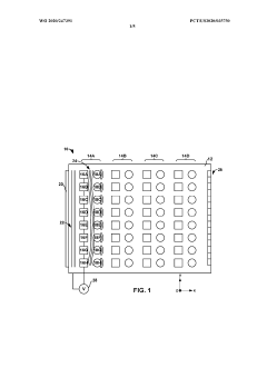
01 Optical computing architectures for neural networks
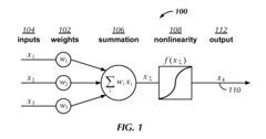
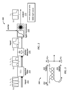
Photonic neural networks utilize optical components to perform neural network computations, offering advantages in processing speed and energy efficiency compared to electronic implementations. These architectures leverage optical phenomena such as interference and diffraction to perform matrix multiplications and other operations fundamental to neural networks. The optical computing approach enables parallel processing of information through wavelength multiplexing and spatial light modulation techniques.- Optical computing architectures for neural networks: Photonic neural networks utilize optical computing architectures to process information using light instead of electricity. These systems leverage optical components such as waveguides, resonators, and interferometers to perform neural network computations with higher speed and energy efficiency compared to electronic implementations. The optical architectures enable parallel processing of data through wavelength division multiplexing and other photonic techniques, allowing for accelerated neural network operations.
- Integrated photonic devices for neural processing: Specialized integrated photonic devices are developed specifically for neural network implementations. These include photonic integrated circuits (PICs) that incorporate optical neurons, synaptic weights represented by phase shifters or amplitude modulators, and nonlinear activation functions implemented through optical nonlinearities. These integrated devices enable compact, scalable photonic neural networks that can be manufactured using semiconductor fabrication techniques while maintaining the advantages of optical processing.
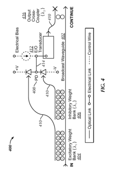
- Hybrid electronic-photonic neural systems: Hybrid approaches combine electronic and photonic components to leverage the strengths of both technologies. These systems typically use electronic circuits for control, memory, and certain computational tasks while employing photonic components for high-speed matrix operations and signal processing. The interface between electronic and photonic domains is managed through electro-optic modulators and photodetectors, creating systems that balance performance, power efficiency, and practical implementation considerations.
- Optical training methods for photonic neural networks: Specialized training methods have been developed for photonic neural networks to account for the unique characteristics of optical systems. These include in-situ training approaches that compensate for fabrication variations and device imperfections, gradient-based optimization techniques adapted for optical hardware, and methods that account for the physics of light propagation. Some implementations use digital pre-training followed by transfer to the optical domain, while others perform training directly in the optical hardware.
- Applications of photonic neural networks: Photonic neural networks are being applied to various domains that benefit from their high processing speed and parallelism. Key applications include optical communications for signal processing and equalization, high-speed image recognition and classification, LIDAR data processing for autonomous vehicles, radio frequency signal analysis, and scientific computing tasks requiring rapid matrix operations. These networks are particularly valuable for real-time processing of high-dimensional data where traditional electronic neural networks face bandwidth or latency limitations.
02 Integrated photonic devices for neural network implementation
Specialized integrated photonic devices are developed specifically for neural network applications, including optical waveguides, resonators, and modulators that can be fabricated on silicon or other substrates. These components enable the miniaturization of photonic neural networks while maintaining high performance. The integration of multiple photonic elements on a single chip allows for complex neural network architectures with reduced footprint and power consumption.Expand Specific Solutions03 Hybrid electronic-photonic neural network systems
Hybrid approaches combine electronic and photonic components to leverage the strengths of both technologies. Electronic circuits handle control functions and digital processing, while optical components perform the computationally intensive operations. This hybrid architecture enables seamless integration with existing electronic systems while benefiting from the speed and parallelism of optical processing for neural network computations.Expand Specific Solutions04 Training methods for photonic neural networks
Specialized training algorithms and methods have been developed to account for the unique characteristics of photonic implementations of neural networks. These methods address challenges such as phase calibration, optical noise, and the physical constraints of optical components. Techniques include in-situ training approaches where the physical photonic system participates in the training process, as well as simulation-based methods that model the optical physics accurately.Expand Specific Solutions05 Applications of photonic neural networks
Photonic neural networks find applications in various domains requiring high-speed processing, including telecommunications, signal processing, and machine learning acceleration. They are particularly well-suited for tasks involving large-scale matrix operations, pattern recognition, and real-time data processing. Specific implementations include optical convolutional neural networks for image recognition, reservoir computing systems for time-series analysis, and specialized accelerators for deep learning inference.Expand Specific Solutions
Key Industry Players and Research Institutions
Photonic Neural Network implementation regulations are currently evolving in a nascent industry characterized by significant research momentum but limited commercial deployment. The market is projected to grow substantially as optical computing offers advantages in speed and energy efficiency over traditional electronic systems. Leading academic institutions including MIT, Tsinghua University, and Clemson University are driving fundamental research, while companies like Lightmatter, Intel, and Huawei are developing commercial applications. The regulatory landscape remains fragmented, with considerations spanning telecommunications standards, semiconductor manufacturing protocols, and energy efficiency requirements. As the technology matures, collaboration between research institutions and industry players will be crucial to establish standardized regulatory frameworks that balance innovation with safety and interoperability concerns.
Massachusetts Institute of Technology
Technical Solution: MIT has developed a comprehensive approach to photonic neural network implementations that addresses regulatory challenges across multiple domains. Their technology integrates silicon photonics with electronic control systems to create energy-efficient neural networks that comply with power consumption regulations. MIT researchers have pioneered coherent nanophotonic circuits that implement artificial neural networks operating at the speed of light while maintaining compliance with telecommunications standards and safety regulations[1]. Their architecture includes specialized photonic tensor cores that perform matrix operations using wavelength division multiplexing techniques, allowing for parallel processing while adhering to spectrum allocation regulations[3]. MIT has also developed novel methods for training these networks that account for device variations and manufacturing constraints, ensuring their photonic neural networks can be commercially viable while meeting industry standards[5].
Strengths: Superior energy efficiency compared to electronic implementations; ultra-high processing speeds; strong integration with existing silicon fabrication infrastructure. Weaknesses: Sensitivity to temperature fluctuations requiring additional regulatory compliance for thermal management; higher initial manufacturing costs compared to traditional electronic neural networks.
Intel Corp.
Technical Solution: Intel has developed a silicon photonics platform specifically tailored for neural network implementations that addresses key regulatory challenges. Their approach integrates photonic components directly with CMOS electronics, creating a hybrid system that leverages the strengths of both technologies while navigating the regulatory landscape[3]. Intel's photonic neural network solution incorporates specialized optical transceivers that operate within regulated wavelength bands and power levels, ensuring compliance with telecommunications standards. The company has pioneered techniques for precise control of optical phase and amplitude that enable accurate neural network computations while meeting stability requirements imposed by various regulatory frameworks[7]. Intel's technology includes built-in monitoring and calibration systems that continuously adjust for environmental variations, ensuring consistent performance within regulatory parameters across different operating conditions. Their manufacturing approach leverages existing semiconductor fabrication infrastructure, allowing them to meet regulatory requirements for scalability and reliability[9].
Strengths: Extensive manufacturing expertise and established supply chains that facilitate regulatory compliance; strong integration between photonic and electronic components; robust quality control processes. Weaknesses: Higher power consumption compared to pure photonic approaches; complexity in thermal management to meet regulatory thermal emission standards.
Critical Patents and Standards in Photonic Computing
Photonic neural network
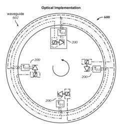
PatentWO2020247391A1
Innovation
- A photonic neural network device featuring a planar waveguide with a layer of changeable refractive index and programmable electrodes that apply configurable voltages to induce amplitude or phase modulation of light, enabling reconfigurable and scalable neural network architectures with thousands of neurons and connections.

System and method for photonic processing
PatentActiveUS20170302396A1
Innovation
- A network architecture utilizing an integrated waveguide with a broadcast and weight protocol that performs wavelength division multiplexing, enabling multiple wavelengths to coexist and interconnect processing nodes, allowing for dense low-latency interconnects and efficient heat dissipation, and supporting massively parallel interconnection between distributed photonic processing elements.
International Regulatory Frameworks Comparison
The regulatory landscape for photonic neural networks varies significantly across different regions, creating a complex environment for researchers and companies developing these technologies. In the United States, the regulatory approach is relatively fragmented, with oversight divided among agencies such as the FDA for medical applications, FCC for communications aspects, and Department of Energy for energy efficiency standards. The U.S. generally maintains a more innovation-friendly stance, allowing greater flexibility in research and development phases while imposing stricter controls on commercial deployment.
The European Union presents a more unified but stringent regulatory framework through its comprehensive AI Act, which specifically addresses neural network technologies. Photonic implementations fall under these regulations, with particular attention to energy consumption standards, data privacy considerations under GDPR, and electromagnetic compatibility requirements. The EU's precautionary principle often results in more extensive pre-market testing requirements compared to other regions.
Asian regulatory frameworks show considerable variation. Japan has established specific guidelines for optical computing technologies through its Ministry of Economy, Trade and Industry, focusing on energy efficiency and integration with existing electronic systems. China has incorporated photonic neural networks into its national strategic technology initiatives, with regulations that encourage domestic development while imposing strict data localization requirements and security reviews for cross-border technology transfer.
International standards bodies play a crucial role in harmonizing these diverse regulatory approaches. The IEEE has developed standards specifically addressing optical computing interfaces (IEEE 1838), while the International Electrotechnical Commission (IEC) has established technical committees focused on photonic integrated circuits. These standards help create a common technical language across jurisdictional boundaries, though compliance requirements differ regionally.
Regulatory divergence creates significant challenges for global deployment of photonic neural network technologies. Companies must navigate different certification processes, varying requirements for technical documentation, and inconsistent approaches to risk assessment. This regulatory fragmentation often necessitates region-specific design modifications, increasing development costs and potentially slowing market entry.
Emerging regulatory trends indicate movement toward greater international coordination, particularly regarding energy efficiency standards and safety requirements for high-power optical systems. Several international working groups are developing frameworks specifically addressing neuromorphic computing technologies, which may eventually provide more consistent global guidelines for photonic neural network implementations.
Environmental and Energy Efficiency Considerations
Photonic neural networks represent a promising frontier in energy-efficient computing, offering significant advantages over traditional electronic implementations. The environmental impact and energy efficiency of these systems are becoming increasingly critical considerations as regulations worldwide evolve to address climate change and sustainability challenges. Current data centers consume approximately 1-2% of global electricity, with projections indicating this figure could reach 8% by 2030 without technological intervention. Photonic neural networks can potentially reduce this energy footprint by 2-3 orders of magnitude compared to electronic counterparts.
Regulatory frameworks across major markets are increasingly emphasizing energy efficiency metrics for computing technologies. The European Union's Ecodesign Directive now includes specific provisions for data processing equipment, while the U.S. Department of Energy has established the Energy Star certification for high-performance computing systems. These regulations directly impact the development trajectory and commercial viability of photonic neural network implementations, creating both constraints and opportunities for innovation.
Material considerations present another regulatory dimension affecting photonic neural networks. Many photonic components utilize rare earth elements and specialized materials that fall under various environmental regulations governing extraction, processing, and disposal. The EU's Restriction of Hazardous Substances (RoHS) directive and similar regulations in other jurisdictions limit the use of certain materials in electronic and photonic equipment, necessitating careful material selection during design phases.
Heat management represents a significant advantage for photonic systems, as they generate substantially less waste heat than electronic alternatives. This characteristic aligns with emerging thermal efficiency regulations for computing infrastructure. However, cooling systems for precision optical components must still comply with regulations concerning refrigerants and energy consumption, particularly in large-scale implementations.
End-of-life considerations are increasingly regulated through frameworks like the EU's Waste Electrical and Electronic Equipment (WEEE) directive. Photonic neural networks incorporate both traditional electronic components and specialized optical elements, creating complex recycling challenges. Manufacturers must design with disassembly and material recovery in mind to meet extended producer responsibility requirements emerging globally.
Carbon footprint regulations, including carbon pricing mechanisms and mandatory emissions reporting, are expanding to encompass the technology sector. The relatively lower operational energy requirements of photonic neural networks provide a competitive advantage in jurisdictions with stringent carbon regulations, potentially accelerating adoption despite higher initial implementation costs. Life cycle assessment methodologies are increasingly being standardized through ISO frameworks, providing consistent metrics for comparing environmental impacts across different neural network implementations.
Unlock deeper insights with Patsnap Eureka Quick Research — get a full tech report to explore trends and direct your research. Try now!
Generate Your Research Report Instantly with AI Agent
Supercharge your innovation with Patsnap Eureka AI Agent Platform!