What Are the Key Material Innovations in Photonic Neural Networks?
OCT 1, 20259 MIN READ
Generate Your Research Report Instantly with AI Agent
Patsnap Eureka helps you evaluate technical feasibility & market potential.
Photonic Neural Networks Background and Objectives
Photonic neural networks represent a revolutionary approach to computing that leverages light rather than electricity to process information. This technology has evolved from the convergence of photonics and neural network architectures, offering promising solutions to the limitations of traditional electronic computing systems. The field traces its origins to the early 2000s when researchers began exploring optical implementations of neural networks, but significant advancements have accelerated in the past decade due to breakthroughs in integrated photonics and machine learning algorithms.
The evolution of photonic neural networks has been driven by the increasing computational demands of artificial intelligence applications and the physical limitations of electronic processors, particularly in terms of energy efficiency and processing speed. Traditional electronic systems face fundamental bottlenecks in power consumption and heat generation as they approach nanoscale dimensions, while photonic systems offer inherent advantages in bandwidth, parallelism, and energy efficiency.
Material innovations have played a crucial role in advancing this technology. Early photonic neural networks relied on bulk optical components, making them impractical for widespread deployment. The development of silicon photonics, lithium niobate on insulator (LNOI), and other integrated photonic platforms has enabled the miniaturization and scalability necessary for practical applications.
The primary technical objectives in this field include achieving higher integration density of photonic components, improving the efficiency and reliability of optical nonlinear elements, developing materials with enhanced electro-optic properties, and creating architectures that effectively leverage the unique capabilities of light for neural computation. Researchers aim to demonstrate photonic neural networks that can outperform electronic counterparts in specific applications while maintaining reasonable power consumption and fabrication costs.
Current research focuses on overcoming several key challenges: developing efficient optical neurons with appropriate nonlinear activation functions, creating high-density and low-loss optical interconnects, implementing precise and programmable optical weights, and integrating photonic systems with electronic control circuitry. Material innovations are central to addressing these challenges, with particular emphasis on materials that exhibit strong optical nonlinearities, low propagation losses, and compatibility with existing fabrication processes.
The long-term vision for photonic neural networks encompasses real-time processing of high-dimensional data streams, ultra-low latency inference for time-critical applications, and energy-efficient computing for edge devices. As material science advances continue to enhance the performance and integration of photonic components, these systems are expected to play an increasingly important role in next-generation computing architectures, particularly for specialized AI acceleration tasks.
Market Analysis for Photonic Computing Solutions
The photonic computing market is experiencing significant growth driven by increasing demands for faster, more energy-efficient computing solutions across various industries. Current market projections indicate that the global photonic computing market is expected to reach $3.8 billion by 2030, with a compound annual growth rate of approximately 32% from 2023 to 2030. This remarkable growth trajectory is primarily fueled by the limitations of traditional electronic computing systems in meeting the computational demands of emerging applications such as artificial intelligence, machine learning, and big data analytics.
The demand for photonic neural networks is particularly strong in data centers, where energy consumption and heat generation have become critical concerns. Data centers currently consume about 1-2% of global electricity, with projections suggesting this could rise to 8% by 2030 without significant efficiency improvements. Photonic computing solutions offer potential energy savings of up to 90% compared to electronic counterparts, making them highly attractive for this sector.
Telecommunications represents another substantial market segment, with network operators seeking solutions to handle exponentially increasing data traffic while minimizing latency and energy consumption. The implementation of 5G and future 6G networks will further accelerate demand for photonic computing technologies capable of processing massive data streams in real-time.
Healthcare and pharmaceutical industries are emerging as promising markets for photonic neural networks, particularly for applications in medical imaging analysis, drug discovery, and genomic sequencing. The market size for AI in healthcare is projected to reach $187 billion by 2030, with photonic computing potentially capturing a significant portion of this growth.
Financial services constitute another key market, where high-frequency trading systems require ultra-low latency processing capabilities that photonic computing can deliver. The competitive advantage gained from even microsecond improvements in transaction speeds represents substantial value in this sector.
Defense and aerospace applications form a smaller but strategically important market segment, with government agencies investing in photonic computing for applications ranging from signal intelligence to autonomous systems. This sector is expected to contribute approximately $500 million to the overall market by 2028.
Regionally, North America currently leads the market with approximately 42% share, followed by Europe (28%) and Asia-Pacific (24%). However, the Asia-Pacific region is expected to demonstrate the highest growth rate over the next decade, driven by substantial investments in advanced computing technologies by countries like China, Japan, and South Korea.
Current State and Challenges in Photonic Materials
Photonic neural networks (PNNs) currently face significant material-related challenges despite their promising potential for high-speed, energy-efficient computing. The field has witnessed substantial progress globally, with research clusters in North America, Europe, and Asia making notable contributions to material innovations.
Silicon photonics remains the dominant material platform due to its compatibility with CMOS fabrication processes, enabling seamless integration with existing semiconductor infrastructure. However, silicon's indirect bandgap limits its light emission capabilities, creating a fundamental bottleneck for fully integrated photonic neural networks. This limitation has spurred research into silicon-compatible materials with enhanced optical properties.
Phase-change materials (PCMs) like Ge₂Sb₂Te₅ (GST) represent a significant advancement, offering non-volatile optical property changes crucial for weight storage in photonic neural networks. These materials can switch between amorphous and crystalline states with dramatically different refractive indices, enabling persistent weight representation without continuous power consumption. Nevertheless, PCMs face challenges including limited switching speed, finite endurance (typically 10⁶-10⁸ cycles), and relatively high power requirements for phase transitions.
Electro-optic materials, particularly lithium niobate (LiNbO₃) and barium titanate (BaTiO₃), have emerged as promising candidates for high-speed modulation in PNNs. Thin-film lithium niobate on insulator (TFLN) technology has dramatically improved electro-optic device performance, achieving modulation bandwidths exceeding 100 GHz. However, integration challenges and fabrication complexities remain significant barriers to widespread adoption.
Two-dimensional materials like graphene and transition metal dichalcogenides (TMDs) offer exceptional electro-optic properties at nanoscale dimensions. Their atomic thinness enables unprecedented miniaturization potential for photonic neural network components. Yet, large-scale fabrication consistency, contact resistance issues, and environmental stability concerns continue to impede commercial viability.
Nonlinear optical materials essential for activation functions in PNNs face particular challenges in achieving sufficient nonlinearity at low optical powers. Current solutions often require either high optical intensities or large device footprints, limiting energy efficiency and integration density. Research into enhanced nonlinear materials, including organic polymers and hybrid organic-inorganic composites, shows promise but remains in early development stages.
Material interfaces and heterogeneous integration represent perhaps the most significant challenge, as optimal PNN performance requires seamless interaction between disparate material systems. Current fabrication techniques struggle with precision alignment, thermal expansion mismatches, and interface quality control at scale, limiting yield and reliability in complex photonic neural network architectures.
Current Material Solutions for Photonic Neural Networks
01 Optical materials for photonic neural networks
Various optical materials are being developed specifically for photonic neural networks to enhance performance and efficiency. These materials include specialized photonic crystals, nonlinear optical materials, and phase-change materials that can modulate light signals effectively. These innovations allow for faster signal processing, reduced energy consumption, and improved computational capabilities in photonic neural network architectures.- Optical materials for photonic neural networks: Various optical materials are being developed specifically for photonic neural networks to enhance their performance. These materials include phase-change materials, nonlinear optical materials, and photonic crystals that can efficiently manipulate light for neural network operations. These specialized materials enable faster signal processing, reduced energy consumption, and improved computational capabilities compared to traditional electronic neural networks.
- Integrated photonic computing architectures: Integrated photonic computing architectures combine multiple photonic components on a single chip to create efficient neural network systems. These architectures incorporate waveguides, resonators, and modulators to process optical signals in parallel. The integration allows for compact designs with high bandwidth capabilities, enabling complex neural network operations while maintaining low power consumption and high processing speeds.
- Neuromorphic photonic processors: Neuromorphic photonic processors mimic the structure and function of biological neural networks using light-based components. These processors utilize specialized materials and structures to implement synaptic weights, activation functions, and network topologies. By leveraging the wave properties of light, these systems can perform complex computations with significantly higher speeds and energy efficiency than conventional electronic neural networks.
- Quantum materials for photonic neural networks: Quantum materials are being explored for their unique properties that can enhance photonic neural networks. These materials exhibit quantum effects such as superposition and entanglement that can be harnessed for neural network operations. Quantum dots, superconducting materials, and topological insulators are being integrated into photonic neural network designs to achieve quantum advantages in computation, potentially enabling more powerful machine learning capabilities.
- Hybrid electronic-photonic neural systems: Hybrid systems that combine electronic and photonic components are being developed to leverage the advantages of both technologies. These systems use electronic components for control and memory functions while utilizing photonic elements for high-speed signal processing and computation. The integration of these complementary technologies allows for versatile neural network implementations that can overcome the limitations of purely electronic or purely photonic approaches.
02 Phase-change materials for programmable photonics
Phase-change materials are emerging as key components in photonic neural networks due to their ability to switch between amorphous and crystalline states. These materials can store and process information through optical properties that change with their phase state. The programmable nature of these materials enables reconfigurable photonic circuits that can adapt to different neural network architectures and learning algorithms, providing versatility in optical computing applications.Expand Specific Solutions03 Integrated photonic platforms for neural computing
Integrated photonic platforms combine various optical components on a single chip to create compact and efficient neural network systems. These platforms incorporate waveguides, resonators, modulators, and detectors fabricated using materials compatible with existing semiconductor manufacturing processes. The integration enables complex neural network architectures while minimizing size, power consumption, and signal loss, making them suitable for edge computing and data center applications.Expand Specific Solutions04 Quantum materials for enhanced photonic processing
Quantum materials with unique optical properties are being explored to enhance the capabilities of photonic neural networks. These materials exhibit quantum effects that can be harnessed for parallel processing and increased computational density. Quantum dots, 2D materials like graphene, and topological insulators are being integrated into photonic neural network designs to achieve quantum advantages in machine learning tasks, potentially enabling computational paradigms beyond classical limitations.Expand Specific Solutions05 Novel fabrication techniques for photonic neural components
Advanced fabrication techniques are being developed to create precise and complex photonic structures needed for neural networks. These include nanoimprint lithography, direct laser writing, and atomic layer deposition methods tailored for optical materials. These techniques enable the creation of three-dimensional photonic structures with sub-wavelength features, precise refractive index control, and multi-material integration, which are essential for implementing efficient optical neural network architectures.Expand Specific Solutions
Leading Organizations in Photonic Computing Industry
Photonic Neural Networks are currently in an early development stage, with the market showing promising growth potential as the technology matures. The global market is expanding as research institutions and companies explore applications in AI acceleration, quantum computing, and telecommunications. Key players like Tsinghua University, Shanghai Jiao Tong University, and Carnegie Mellon University are leading academic research, while companies such as Eastman Kodak and Futurewei Technologies are developing commercial applications. Material innovations remain a critical focus area, with Zhejiang University, University of Washington, and National University of Singapore making significant advances in photonic materials. The technology is approaching commercial viability, with early adopters emerging in high-performance computing and telecommunications sectors where traditional electronic systems face limitations.
University of Washington
Technical Solution: The University of Washington has developed groundbreaking material platforms for photonic neural networks centered around lithium niobate (LiNbO3) thin films and novel 2D materials. Their research team has pioneered techniques to create ultra-thin LiNbO3 films with exceptional electro-optic properties, enabling high-speed optical modulators that form the backbone of their photonic neural network architecture. These thin-film structures achieve modulation speeds exceeding 100 GHz while maintaining low optical losses. Additionally, they've integrated 2D materials like graphene and transition metal dichalcogenides (TMDs) to create tunable photonic synapses with analog weight control. Their hybrid material approach combines the strong electro-optic effects of LiNbO3 with the unique optoelectronic properties of 2D materials, resulting in photonic neural networks that demonstrate reconfigurable functionality with minimal power consumption. Recent demonstrations include a photonic convolutional neural network processor that achieved image classification tasks with 95% accuracy while consuming only milliwatts of power.
Strengths: Lithium niobate platform offers exceptional electro-optic properties with high-speed modulation capabilities. Integration of 2D materials provides additional functionality and tunability. Weaknesses: Complex fabrication processes involving multiple material systems may present challenges for large-scale manufacturing and integration.
National University of Singapore
Technical Solution: National University of Singapore (NUS) has developed innovative material solutions for photonic neural networks focusing on perovskite-based photonic computing elements. Their research team has engineered halide perovskite materials with exceptional optoelectronic properties that enable efficient all-optical neural network implementations. These materials exhibit strong optical nonlinearities, tunable bandgaps, and can be solution-processed for cost-effective manufacturing. NUS researchers have demonstrated perovskite-based optical neurons that can perform weighted summation and nonlinear activation functions entirely in the optical domain. Their material platform incorporates compositionally engineered perovskites (CsPbX3 and MAPbX3 variants) that achieve ultrafast optical response times in the picosecond range while maintaining stability under operating conditions. The university has also pioneered hybrid integration techniques that combine these perovskite materials with silicon photonics platforms, enabling scalable photonic neural network architectures. Recent demonstrations include an all-optical matrix multiplication unit that achieves computation speeds thousands of times faster than electronic implementations while consuming orders of magnitude less energy.
Strengths: Perovskite materials offer exceptional optical properties with solution processability for cost-effective manufacturing. Ultrafast optical response enables extremely high-speed neural network operations. Weaknesses: Perovskite materials still face challenges with long-term stability and environmental sensitivity, potentially requiring additional encapsulation or protection strategies.
Key Material Innovations and Patent Analysis
Method and apparatus for training a neural network
PatentPendingUS20250200351A1
Innovation
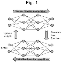
- A method of training neural networks where a mathematically linear stage of the forward propagation is performed optically, allowing for direct incorporation of optical signal updates into the weight matrices, thereby enhancing hybrid training and reducing the reality gap.
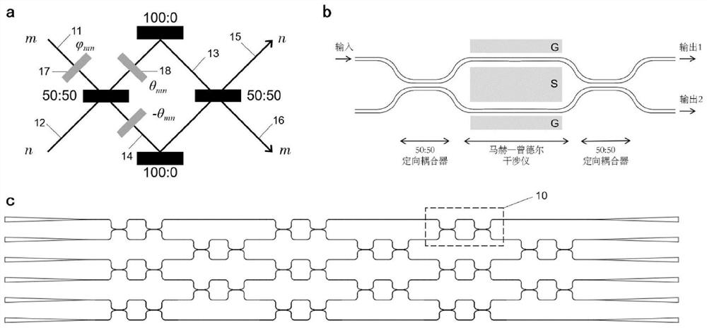
On-chip cascaded MZI reconfigurable quantum network based on lithium niobate
PatentPendingCN111898741A
Innovation
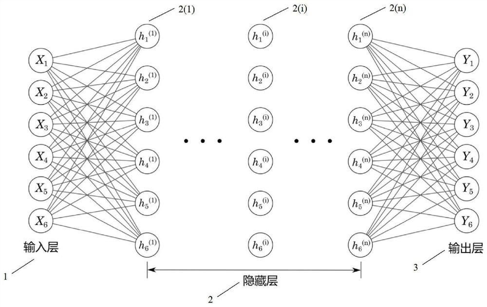
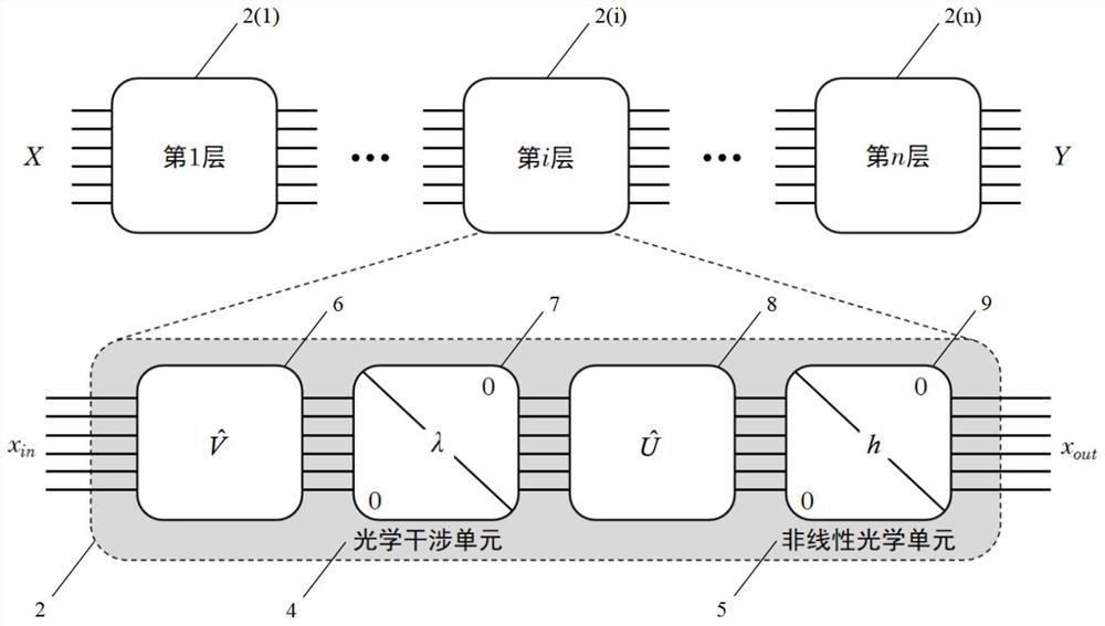
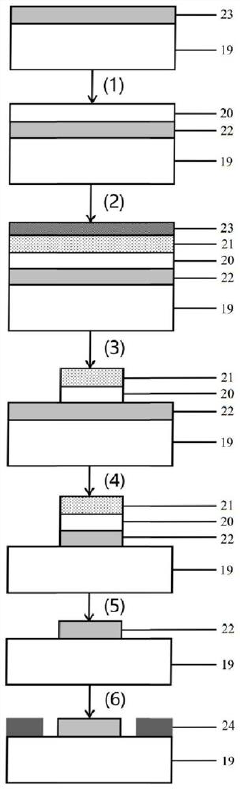
- An on-chip cascaded Mach-Zehnder interferometer (MZI) based on lithium niobate is used to reconfigurable quantum network architecture, including an input waveguide array, MZI, saturable absorber array and detector array, through optical interference and nonlinear optical units Realize quantum optical neural network, use lithium niobate thin film to prepare Mach-Zehnder interferometer, and combine plasma-enhanced chemical deposition, electron beam lithography and reactive ion etching technology.
Energy Efficiency Comparison with Electronic Systems
Photonic neural networks (PNNs) demonstrate significant advantages in energy efficiency compared to their electronic counterparts, representing a critical factor driving their development. Traditional electronic neural networks face fundamental energy limitations due to resistive heating and interconnect bottlenecks, particularly as computational demands increase. In contrast, PNNs leverage the inherent parallelism and low-loss transmission characteristics of light to achieve superior energy performance.
Quantitative analyses reveal that photonic implementations can achieve energy efficiencies in the femtojoule per operation range, representing orders of magnitude improvement over electronic systems. For instance, recent experimental demonstrations have shown that photonic matrix multiplication operations can be performed with energy consumption as low as 10-15 joules per multiply-accumulate operation, compared to 10-12 joules in advanced electronic systems.
The energy advantage stems from several fundamental physical principles. First, photons do not interact with each other in linear optical media, eliminating crosstalk issues that plague electronic systems. Second, wavelength division multiplexing enables multiple signals to be processed simultaneously without additional energy costs. Third, the propagation of optical signals through waveguides incurs minimal energy loss compared to electron movement through resistive electronic interconnects.
Temperature management represents another significant advantage for photonic systems. Electronic neural networks generate substantial heat during operation, requiring elaborate cooling systems that consume additional energy. Photonic systems generate significantly less heat, reducing cooling requirements and associated energy costs. This becomes particularly important in data center environments where cooling can represent up to 40% of total energy consumption.
When scaling to large neural network architectures, the energy efficiency gap widens further. Electronic systems face a quadratic increase in energy consumption with network size due to interconnect challenges, while photonic systems maintain more favorable scaling properties. Recent studies project that for large-scale deep learning applications, mature photonic neural networks could potentially operate with 100-1000x better energy efficiency than their electronic counterparts.
However, these comparisons must account for the full system energy budget, including laser sources, photodetectors, and electronic-photonic conversion overhead. Current hybrid electronic-photonic systems still face efficiency challenges at these interfaces, though ongoing research in integrated laser sources and efficient modulators continues to address these limitations.
Manufacturing Scalability and Integration Challenges
The manufacturing scalability and integration of photonic neural networks (PNNs) represent significant hurdles in their widespread adoption. Current fabrication techniques for photonic integrated circuits (PICs) face substantial challenges when attempting to scale to the complexity required for neural network implementations. The primary limitation stems from the precision requirements for waveguide dimensions, where nanometer-scale variations can significantly impact optical performance and introduce computational errors in neural network operations.
Silicon photonics platforms, while benefiting from compatibility with CMOS manufacturing infrastructure, encounter yield issues when scaling beyond certain complexity thresholds. The integration density of photonic components remains orders of magnitude lower than their electronic counterparts, limiting the neural network size that can be practically implemented on a single chip. This density limitation is particularly problematic for deep learning architectures that require millions of parameters.
Material uniformity across large wafers presents another critical challenge. Phase-change materials and nonlinear optical materials, which are essential for implementing tunable weights in photonic neural networks, often exhibit composition variations that affect their optical properties. These variations translate directly into weight uncertainties in the neural network, potentially degrading computational accuracy and training convergence.
Thermal management emerges as a significant integration challenge as photonic neural networks scale up. Many photonic weight elements rely on thermo-optic effects for tuning, creating substantial heat loads that must be efficiently dissipated. Current cooling solutions become inadequate at higher integration densities, limiting operational speeds and reliability.
The interface between electronic control circuitry and photonic components represents a persistent bottleneck. While the photonic elements can process data at extremely high speeds, the electronic drivers and readout circuits often cannot match this performance. This electronic-photonic interface requires sophisticated co-design approaches and potentially new material systems that can bridge the performance gap.
Packaging solutions for photonic neural networks remain underdeveloped compared to electronic systems. Fiber-to-chip coupling efficiency, alignment tolerance, and environmental stability all present significant challenges. The need for precise optical alignment increases assembly costs and reduces manufacturing throughput, creating barriers to mass production.
Recent advances in heterogeneous integration, combining different material platforms through wafer bonding or transfer printing, show promise for overcoming some of these limitations. However, these approaches introduce additional process complexity and potential reliability concerns that must be addressed before industrial-scale manufacturing becomes viable.
Unlock deeper insights with Patsnap Eureka Quick Research — get a full tech report to explore trends and direct your research. Try now!
Generate Your Research Report Instantly with AI Agent
Supercharge your innovation with Patsnap Eureka AI Agent Platform!