How Photonic Neural Networks Drive Innovation in Sensor Technologies?
OCT 1, 202510 MIN READ
Generate Your Research Report Instantly with AI Agent
Patsnap Eureka helps you evaluate technical feasibility & market potential.
Photonic Neural Networks Background and Objectives
Photonic neural networks represent a revolutionary approach to computing that leverages light rather than electricity to process information. This technology has evolved from the convergence of photonics and neural network architectures, offering unprecedented advantages in processing speed, energy efficiency, and bandwidth capacity. The historical trajectory of photonic neural networks began in the late 1980s with optical computing concepts, but significant advancements have only materialized in the past decade due to breakthroughs in integrated photonics, nanofabrication techniques, and machine learning algorithms.
The evolution of this technology has been driven by the fundamental limitations of electronic computing systems, particularly in terms of speed and energy consumption. Traditional electronic neural networks face bottlenecks in data transfer and processing speeds, while photonic implementations can potentially operate at the speed of light with minimal energy dissipation. This paradigm shift addresses critical challenges in real-time data processing for emerging applications such as autonomous vehicles, advanced medical diagnostics, and environmental monitoring systems.
Current technological trends indicate a rapid acceleration in photonic neural network development, with particular emphasis on their integration with sensor technologies. The synergy between photonic neural networks and sensors creates opportunities for edge computing architectures that can process sensory data with minimal latency and power requirements. This integration enables real-time analysis and decision-making capabilities that were previously unattainable with conventional electronic systems.
The primary technical objectives in this field include developing scalable photonic neural network architectures that can be manufactured using standard semiconductor processes, reducing optical loss in integrated photonic circuits, and creating efficient interfaces between electronic and photonic components. Additionally, researchers aim to develop specialized training algorithms optimized for the unique characteristics of photonic neural networks, as traditional backpropagation methods may not directly translate to optical systems.
From a sensor technology perspective, the integration with photonic neural networks aims to achieve ultra-fast signal processing, enhanced sensitivity across multiple spectral ranges, and intelligent feature extraction directly from raw sensor data. These capabilities would enable next-generation sensing applications with unprecedented performance in challenging environments, such as detecting trace chemicals in complex mixtures, identifying subtle patterns in biological signals, or performing real-time object recognition in dynamic scenes.
The convergence of photonic neural networks and sensor technologies represents a transformative opportunity to overcome current limitations in data acquisition and processing, potentially revolutionizing fields ranging from healthcare diagnostics to industrial automation and environmental monitoring.
Market Demand Analysis for Advanced Sensing Solutions
The global market for advanced sensing solutions is experiencing unprecedented growth, driven by the convergence of photonic neural networks and sensor technologies. Current market analysis indicates that the demand for high-precision, real-time sensing capabilities is expanding across multiple industries, including healthcare, automotive, industrial automation, and environmental monitoring. This surge is primarily attributed to the increasing need for more efficient data processing at the edge, reduced latency in critical applications, and lower power consumption in IoT devices.
In the healthcare sector, advanced photonic sensors are revolutionizing diagnostic capabilities through non-invasive monitoring systems and point-of-care devices. The integration of photonic neural networks enables these sensors to detect biomarkers with significantly higher sensitivity than conventional methods, creating substantial market opportunities for early disease detection and personalized medicine applications.
The automotive industry represents another significant market segment, with autonomous vehicles requiring sophisticated sensor arrays capable of processing environmental data instantaneously. Traditional electronic sensors face limitations in processing speed and power efficiency that photonic neural network-based solutions can overcome, offering enhanced object recognition and situational awareness even in adverse weather conditions.
Industrial IoT applications constitute a rapidly growing market segment for advanced sensing technologies. Manufacturing facilities are increasingly adopting smart sensors for predictive maintenance, quality control, and process optimization. The ability of photonic neural networks to process complex spectral data in real-time provides unprecedented capabilities for detecting material anomalies and equipment failures before they occur, significantly reducing downtime and operational costs.
Environmental monitoring represents another expanding market, with governments and organizations worldwide investing in advanced sensing networks to track air quality, water contamination, and climate indicators. Photonic neural network-enabled sensors offer superior capabilities in detecting trace elements and analyzing complex environmental data patterns, supporting more effective conservation efforts and regulatory compliance.
Market forecasts suggest that miniaturization and cost reduction will be critical factors driving wider adoption of photonic neural network-based sensing solutions. As manufacturing techniques evolve and economies of scale take effect, these advanced sensors are expected to penetrate consumer electronics markets, creating new applications in wearable health monitoring, smart home systems, and personal security devices.
The market is also witnessing increasing demand for integrated sensing solutions that combine multiple sensing modalities with on-device intelligence. This trend aligns perfectly with the capabilities of photonic neural networks, which can efficiently process diverse data types simultaneously, offering comprehensive environmental awareness through a single integrated platform.
Current State and Challenges in Photonic Neural Networks
Photonic neural networks (PNNs) represent a significant advancement in the field of neuromorphic computing, combining principles of optics and neural networks to create systems that process information at the speed of light. Currently, these networks are being developed across various research institutions and technology companies worldwide, with notable progress in North America, Europe, and Asia. The fundamental architecture of PNNs leverages optical interference, nonlinear materials, and waveguide technologies to perform neural network computations with photons rather than electrons.
The current state of PNN technology demonstrates several promising advantages over traditional electronic neural networks. These include ultra-high processing speeds (potentially reaching terahertz frequencies), significantly lower power consumption, and the ability to perform parallel computations naturally through wavelength division multiplexing. Early prototypes have shown the capability to perform basic pattern recognition tasks and signal processing operations with remarkable efficiency, particularly in applications requiring real-time processing of high-dimensional data.
Despite these advancements, PNNs face substantial technical challenges that limit their widespread adoption. One primary obstacle is the integration of efficient optical nonlinearities that can operate at low power levels. Current nonlinear optical materials often require high optical intensities to exhibit the necessary nonlinear effects, limiting energy efficiency and scalability. Additionally, the fabrication of photonic integrated circuits with the precision required for neural network operations presents significant manufacturing challenges.
Temperature sensitivity remains another critical issue, as many photonic components exhibit performance variations with temperature fluctuations, affecting the stability and reliability of PNNs in real-world environments. The lack of standardized design methodologies and simulation tools specifically tailored for photonic neural architectures further complicates development efforts.
The interface between electronic and photonic domains represents a significant bottleneck, with current electro-optical and opto-electronic conversion processes introducing latency and energy overhead that can negate some of the inherent advantages of photonic processing. This challenge is particularly relevant for sensor applications where data originates in the electronic domain.
From a geographical perspective, research leadership in PNNs is distributed across several regions. North American institutions and companies lead in fundamental research and theoretical frameworks, while European entities excel in photonic integration technologies. Asian research groups, particularly in China and Japan, have made significant contributions to materials science aspects of PNNs and practical implementations.
The current technological landscape also reveals a gap between laboratory demonstrations and commercially viable products, with most PNN implementations remaining at the proof-of-concept stage. Bridging this gap requires addressing not only the technical challenges but also developing manufacturing processes that enable cost-effective production at scale.
Current Photonic Neural Network Implementations for Sensing
01 Optical computing architectures for neural networks
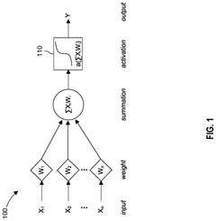
Photonic neural networks leverage optical computing architectures to process information using light instead of electricity. These systems utilize optical components such as waveguides, resonators, and interferometers to perform neural network computations with higher speed and energy efficiency compared to electronic systems. The optical architectures enable parallel processing of data through wavelength multiplexing and can implement various neural network operations including matrix multiplication and activation functions through photonic circuits.- Optical computing architectures for neural networks: Photonic neural networks leverage optical computing architectures to process information using light rather than electricity. These systems utilize optical components such as waveguides, resonators, and interferometers to perform neural network computations with significantly higher speed and energy efficiency compared to electronic implementations. The architecture enables parallel processing of multiple wavelengths of light, allowing for complex matrix operations essential for neural network functionality.
- Integrated photonic processors for AI applications: Integrated photonic processors combine multiple optical components on a single chip to create compact, efficient neural network systems. These processors incorporate photonic integrated circuits (PICs) that enable complex neural network operations through manipulation of light signals. The integration allows for reduced footprint, lower power consumption, and enhanced processing capabilities for artificial intelligence applications, including image recognition, natural language processing, and data analytics.
- Optical-electronic hybrid neural network systems: Hybrid neural network systems combine the advantages of both photonic and electronic processing. These systems use optical components for high-speed matrix operations and data transmission while leveraging electronic components for control, memory, and specific computational tasks. The hybrid approach addresses limitations of purely optical systems, such as memory storage, while maintaining the speed and energy efficiency benefits of photonic processing for large-scale neural network operations.
- Novel photonic materials and components for neural networks: Advanced materials and components are being developed specifically for photonic neural networks, including phase-change materials, nonlinear optical materials, and specialized photonic structures. These innovations enable more efficient light manipulation, improved signal processing, and enhanced computational capabilities. Novel components such as optical neurons, photonic synapses, and specialized waveguides allow for more complex neural network architectures and learning capabilities within the optical domain.
- Training and optimization methods for photonic neural networks: Specialized algorithms and techniques have been developed for training and optimizing photonic neural networks. These methods address the unique challenges of optical systems, including phase sensitivity, noise management, and hardware constraints. Innovations include in-situ training approaches, hardware-aware learning algorithms, and techniques for converting traditional neural network models to efficient photonic implementations while maintaining accuracy and performance.
02 Integrated photonic neural network hardware
Integrated photonic devices implement neural network functionalities directly in hardware using photonic integrated circuits (PICs). These systems incorporate specialized components such as optical modulators, photodetectors, and phase shifters on silicon or other substrates to create compact neural network processors. The integration enables miniaturization of photonic neural networks while maintaining high processing speeds and reducing power consumption, making them suitable for edge computing applications and AI accelerators.Expand Specific Solutions03 Hybrid electronic-photonic neural systems
Hybrid approaches combine electronic and photonic technologies to leverage the advantages of both domains. These systems typically use electronic components for control and memory while employing photonic elements for high-speed computation and data transmission. The hybrid architecture allows for seamless integration with existing electronic infrastructure while benefiting from the speed and parallelism of optical processing. This approach addresses challenges in interfacing between electronic and photonic domains and provides a practical pathway for adoption of photonic neural networks.Expand Specific Solutions04 Neuromorphic photonic computing
Neuromorphic photonic systems mimic the structure and function of biological neural networks using optical components. These systems implement spiking neural networks and other brain-inspired architectures through photonic elements that emulate neuronal and synaptic behaviors. By utilizing the wave properties of light, these systems can perform complex computational tasks with high energy efficiency. Neuromorphic photonic computing enables new approaches to machine learning that are particularly suited for pattern recognition, signal processing, and real-time data analysis.Expand Specific Solutions05 Novel materials and fabrication techniques for photonic neural networks
Advanced materials and fabrication methods enable new capabilities in photonic neural networks. These include phase-change materials, nonlinear optical materials, and specialized photonic structures that enhance the performance of optical neural networks. Novel fabrication techniques allow for precise control of optical properties and integration of multiple functionalities within compact devices. These innovations address challenges in scalability, energy efficiency, and manufacturing of photonic neural network components, paving the way for practical applications in various fields including telecommunications, sensing, and artificial intelligence.Expand Specific Solutions
Key Industry Players in Photonic Neural Networks
Photonic Neural Networks in sensor technologies are evolving rapidly, currently transitioning from research to early commercialization. The market is projected to grow significantly as applications expand across autonomous systems, healthcare, and telecommunications. Technology maturity varies among key players: established corporations like Hewlett Packard Enterprise, Microsoft, and Applied Materials are advancing commercial applications, while academic institutions (MIT, Harvard, National University of Singapore) drive fundamental research. Specialized companies like Lightmatter and SRI International are developing targeted solutions. Semiconductor manufacturers including TSMC, SMIC, and Sony are integrating photonic neural networks into existing sensor platforms, creating a competitive landscape where collaboration between research institutions and industry is accelerating innovation and market adoption.
Hewlett Packard Enterprise Development LP
Technical Solution: HPE has developed an optical computing architecture called "Memory-Driven Computing" that incorporates photonic neural networks for sensor data processing. Their approach uses silicon photonics to create optical interconnects between computing nodes and memory, significantly reducing the energy required for data movement. For neural network implementations, HPE employs a hybrid electro-optical approach where optical components handle the interconnect and communication while specialized electronic circuits perform the computational functions. Their photonic neural network technology features reconfigurable optical meshes that can be programmed to implement different neural network topologies optimized for specific sensor applications. HPE has demonstrated systems capable of processing sensor data streams at rates exceeding 10 Tbps with power efficiency improvements of over 20x compared to electronic-only implementations. A key innovation is their "Sensor-to-Insight" architecture that enables direct optical interfaces with various sensor types, allowing sensor data to remain in the optical domain throughout much of the processing pipeline, minimizing energy-intensive optical-electronic conversions.
Strengths: Enterprise-grade implementation with focus on practical deployment scenarios; Strong integration with existing data center infrastructure; Comprehensive approach addressing both computation and data movement. Weaknesses: Less specialized for edge sensor applications compared to pure-play photonic neural network companies; Hybrid approach may not achieve the theoretical maximum performance of pure photonic implementations.
The Regents of the University of California
Technical Solution: The University of California system has developed several pioneering technologies in photonic neural networks for sensor applications across its campuses. UC Berkeley and UC San Diego have been particularly active in this field, creating integrated photonic platforms that combine phase-change materials with silicon photonics to implement neural network operations. Their architecture employs wavelength division multiplexing to perform parallel matrix operations using arrays of Mach-Zehnder interferometers and microring resonators. For sensor applications, UC researchers have demonstrated photonic neural networks capable of processing data from multiple sensor modalities simultaneously, including optical, RF, and acoustic sensors. A key innovation is their development of programmable photonic tensor cores that can be reconfigured in real-time to adapt to different sensing tasks. UC Santa Barbara has pioneered heterogeneous integration approaches that combine III-V materials with silicon photonics to create efficient optical sources and detectors integrated with photonic neural network processors. Their systems have demonstrated processing capabilities exceeding 100 TOPS/W for sensor data analytics, with latencies in the nanosecond range.
Strengths: Broad research portfolio covering multiple aspects of photonic neural networks; Strong focus on heterogeneous integration for practical implementation; Demonstrated capabilities across diverse sensor types. Weaknesses: Research distributed across multiple campuses may lack unified commercialization strategy; Some approaches require specialized fabrication techniques not yet widely available in commercial foundries.
Core Innovations in Photonic Neural Network Architecture
Photonic neural network
PatentActiveUS12340301B2
Innovation
- A photonic neural network device featuring a planar waveguide, a layer with a changeable refractive index, and programmable electrodes that apply configurable voltages to induce amplitude or phase modulation of light, enabling reconfigurable and scalable neural network architecture.
On-chip laser neuron integrated on silicon
PatentPendingUS20240311627A1
Innovation
- An all-optical nonlinear activation function is integrated directly on a common substrate with a photonic neural network using a hybrid Group III-V-on-Si platform, featuring an optically active region within a resonator cavity, enabling energy-efficient and high-bandwidth data processing by generating optical signals through stimulated emission.
Energy Efficiency and Sustainability Considerations
Photonic neural networks represent a significant advancement in energy-efficient computing architectures, offering substantial sustainability benefits when applied to sensor technologies. The integration of photonics with neural networks fundamentally transforms the energy consumption profile of sensing systems by leveraging light's inherent properties for computation rather than electricity. Traditional electronic sensor systems require multiple energy-intensive conversion steps between optical and electronic domains, whereas photonic neural networks can process optical signals directly, eliminating these conversion losses.
Energy efficiency metrics for photonic neural network-based sensors demonstrate remarkable improvements, with some implementations showing 100-1000x reduction in power consumption compared to their electronic counterparts. This efficiency stems from the near-zero heat generation during optical signal propagation and processing, contrasting sharply with the significant thermal management challenges faced by electronic systems.
The sustainability impact extends beyond operational energy savings. Photonic components typically have longer operational lifespans than electronic equivalents, reducing replacement frequency and associated electronic waste. Additionally, many photonic materials have lower environmental extraction and processing costs than rare earth elements commonly used in advanced electronics.
Carbon footprint analyses of sensor networks implementing photonic neural networks reveal potential for significant greenhouse gas emission reductions across industrial monitoring applications. For instance, smart manufacturing facilities utilizing photonic neural network sensors for quality control can reduce their sensing-related carbon emissions by up to 60% while maintaining or improving detection accuracy.
From a lifecycle perspective, photonic neural network sensors present compelling sustainability advantages. While initial fabrication may require specialized processes, the extended operational lifetime and reduced energy demands create favorable total environmental impact profiles. The integration of these systems into renewable energy monitoring applications creates a virtuous cycle, where energy-efficient sensors improve the performance of clean energy systems.
Regulatory frameworks are increasingly recognizing these sustainability benefits, with several jurisdictions developing incentive programs for low-power sensing technologies. Industry standards bodies are also establishing certification pathways specifically for energy-efficient sensing systems, creating market advantages for photonic neural network implementations.
As climate considerations become more central to technology deployment decisions, the inherent energy efficiency of photonic neural networks positions them as a key enabling technology for sustainable sensing infrastructure across multiple sectors including environmental monitoring, industrial automation, and smart city applications.
Integration Challenges with Existing Sensor Infrastructure
The integration of photonic neural networks (PNNs) with existing sensor infrastructure presents significant technical challenges that must be addressed to realize their full potential in next-generation sensing applications. Current sensor ecosystems have been developed around electronic processing paradigms, creating compatibility issues when introducing photonic-based neural processing. The primary challenge lies in the interface between conventional electronic sensors and photonic neural networks, which requires complex signal transduction mechanisms to convert electronic signals to optical formats and vice versa.
Hardware compatibility represents a major hurdle, as most deployed sensor systems lack the necessary optical interfaces for direct integration with PNNs. This necessitates the development of hybrid electronic-photonic interfaces that can efficiently bridge this gap without introducing excessive latency or signal degradation. These interfaces must maintain signal integrity while managing the fundamental differences in how information is encoded and processed between electronic and photonic domains.
Power requirements present another significant integration challenge. While PNNs offer theoretical energy efficiency advantages for certain operations, the conversion processes between electronic and photonic domains can introduce energy overhead that may offset these benefits in practical implementations. Existing sensor infrastructure typically operates within strict power budgets that may be incompatible with the requirements of first-generation photonic neural network systems.
Data protocol standardization remains underdeveloped for photonic neural network integration. Current sensor networks utilize well-established electronic communication protocols that lack direct photonic equivalents. The absence of standardized interfaces for photonic neural processing creates significant barriers to widespread adoption and interoperability across different sensor platforms and manufacturers.
Physical space constraints in existing sensor deployments also limit integration possibilities. Many current sensor applications prioritize miniaturization, while early photonic neural network implementations require relatively large footprints for waveguides, modulators, and other optical components. This size mismatch creates practical deployment challenges, particularly in space-constrained applications like wearable technology or distributed IoT sensor networks.
Temperature sensitivity presents additional integration difficulties, as photonic components often require more stringent environmental controls than their electronic counterparts. Many existing sensor deployments operate in variable temperature environments that could compromise the performance of photonic neural networks without additional thermal management systems, which would further increase system complexity and cost.
Unlock deeper insights with Patsnap Eureka Quick Research — get a full tech report to explore trends and direct your research. Try now!
Generate Your Research Report Instantly with AI Agent
Supercharge your innovation with Patsnap Eureka AI Agent Platform!