How does bandgap engineering affect Photoelectrochemical Water Splitting?
SEP 4, 20259 MIN READ
Generate Your Research Report Instantly with AI Agent
Patsnap Eureka helps you evaluate technical feasibility & market potential.
Bandgap Engineering Background and Objectives
Bandgap engineering has emerged as a pivotal approach in the development of efficient photoelectrochemical (PEC) water splitting systems over the past several decades. This technology represents a promising pathway toward sustainable hydrogen production using solar energy, addressing global energy challenges while minimizing environmental impact. The fundamental principle behind PEC water splitting involves the absorption of photons by semiconductor materials to generate electron-hole pairs, which subsequently drive water oxidation and reduction reactions.
The evolution of bandgap engineering in this field can be traced back to the 1970s when Fujishima and Honda first demonstrated photocatalytic water splitting using TiO2. Since then, significant advancements have been made in understanding how the electronic structure of semiconductors affects their performance in PEC systems. The field has progressed from simple single-semiconductor systems to complex architectures involving multiple materials with engineered bandgaps.
Current technological trends indicate a shift toward nanostructured materials, heterojunctions, and quantum-confined systems that allow precise control over bandgap properties. These approaches enable researchers to overcome the inherent limitations of individual semiconductors by creating synergistic combinations that address multiple aspects of the water-splitting process simultaneously. The integration of computational modeling with experimental techniques has accelerated this progress, allowing for more targeted design of materials with optimal bandgap configurations.
The primary technical objective in this domain is to develop semiconductor systems with bandgaps that efficiently harvest the solar spectrum while maintaining sufficient energy to drive the water-splitting reaction. This requires a delicate balance, as the theoretical minimum bandgap for water splitting is 1.23 eV, but practical systems typically require 1.8-2.0 eV due to overpotential requirements and energy losses. Additionally, engineered materials must demonstrate long-term stability in aqueous environments and cost-effectiveness for large-scale implementation.
Another critical objective is to address the mismatch between light absorption and charge carrier properties. Many materials with ideal bandgaps for solar absorption suffer from poor charge transport characteristics or rapid recombination rates. Bandgap engineering aims to decouple these properties through strategies such as doping, alloying, and creating heterojunctions, allowing for independent optimization of light harvesting and charge separation processes.
Looking forward, the field is moving toward achieving solar-to-hydrogen conversion efficiencies exceeding 10% with stability over thousands of hours, which would represent a significant milestone for commercial viability. This requires innovative approaches to bandgap engineering that can simultaneously address efficiency, stability, and scalability challenges that have historically limited widespread adoption of PEC water splitting technology.
Market Analysis for PEC Water Splitting Technologies
The global market for photoelectrochemical (PEC) water splitting technologies is experiencing significant growth, driven by increasing demand for clean hydrogen production methods. Current market valuations indicate that the hydrogen generation market is expected to reach $220 billion by 2030, with PEC water splitting technologies potentially capturing 15-20% of this market in the long term. The compound annual growth rate (CAGR) for PEC technologies specifically is projected at 12.7% through 2028, outpacing traditional hydrogen production methods.
Regional analysis reveals that Asia-Pacific currently dominates the PEC water splitting market, with China, Japan, and South Korea making substantial investments in research and commercialization. Europe follows closely, particularly with strong government backing in Germany, France, and the Nordic countries through initiatives like the European Hydrogen Strategy. North America shows promising growth potential, especially with recent policy shifts favoring green hydrogen technologies.
Market segmentation indicates that bandgap-engineered photocatalysts represent approximately 35% of the current PEC technology market, with this share expected to increase to 45% by 2025. This growth is directly attributable to the enhanced efficiency and durability that bandgap engineering provides to PEC systems, allowing for broader spectrum utilization and improved solar-to-hydrogen conversion rates.
End-user industries driving demand include renewable energy storage (42%), industrial chemical production (28%), transportation fuel (18%), and decentralized power generation (12%). The industrial chemical sector is showing the fastest growth rate at 16.3% annually, as companies seek to decarbonize their hydrogen feedstock sources.
Investment patterns reveal increasing venture capital interest, with funding for bandgap engineering startups in PEC technologies growing from $120 million in 2018 to over $450 million in 2022. Corporate R&D spending in this sector has similarly increased by approximately 22% year-over-year since 2020.
Market barriers include high initial capital costs, with current levelized cost of hydrogen (LCOH) from PEC systems ranging from $5-8/kg compared to $1-3/kg for conventional methods. However, cost projections suggest PEC technologies could achieve cost parity by 2028-2030, primarily through advances in bandgap engineering that improve efficiency and reduce material costs.
Consumer adoption trends indicate growing acceptance of hydrogen as an energy carrier, with 68% of industrial users expressing willingness to pay premium prices for green hydrogen produced through solar water splitting technologies, representing a significant market opportunity for advanced PEC systems utilizing bandgap engineering innovations.
Current Challenges in Bandgap Engineering for PEC Systems
Despite significant advancements in photoelectrochemical (PEC) water splitting technology, bandgap engineering continues to face substantial challenges that impede widespread commercial implementation. The fundamental trade-off between light absorption and electrochemical potential remains a critical bottleneck. Materials with narrow bandgaps efficiently harvest visible light but often lack sufficient potential to drive water-splitting reactions, while wide-bandgap semiconductors provide adequate potential but utilize only a small portion of the solar spectrum.
Material stability presents another significant hurdle, particularly for high-performance semiconductors. Many promising materials with optimal bandgaps suffer from photocorrosion or degradation under operational conditions. This instability is especially pronounced in materials engineered for visible light absorption, where the electronic structure modifications that enhance light harvesting frequently compromise chemical stability in aqueous electrolytes.
Charge carrier dynamics in engineered bandgap materials often exhibit suboptimal behavior. The introduction of dopants, alloying elements, or heterojunctions—while beneficial for bandgap tuning—frequently creates recombination centers that diminish quantum efficiency. The complex interplay between bandgap narrowing and charge carrier lifetime represents a persistent engineering challenge requiring sophisticated material design strategies.
Manufacturing scalability poses substantial barriers to commercial deployment. Many advanced bandgap engineering techniques, such as quantum confinement structures, epitaxial growth, and precision doping, rely on expensive, energy-intensive processes with low throughput. The translation of laboratory-scale bandgap engineering achievements to industrially viable production methods remains largely unresolved.
Interface engineering at semiconductor-electrolyte boundaries presents unique challenges for bandgap-engineered materials. Band edge positions must align appropriately with water redox potentials while maintaining favorable interfacial charge transfer kinetics. Surface states and reconstruction phenomena often compromise the theoretical advantages gained through bandgap optimization in bulk materials.
Computational prediction limitations further complicate progress. Despite advances in density functional theory and other modeling approaches, accurately predicting the properties of complex, doped, or nanostructured materials remains difficult. The gap between theoretical predictions and experimental outcomes frequently necessitates resource-intensive trial-and-error approaches to bandgap engineering.
Economic viability concerns persist as well. The cost-performance ratio of bandgap-engineered PEC systems must compete with alternative hydrogen production technologies. Current materials that meet technical requirements often incorporate expensive elements like platinum-group metals or complex fabrication processes, raising questions about long-term economic sustainability.
Current Bandgap Modification Strategies and Materials
01 Bandgap engineering for semiconductor materials
Bandgap engineering involves modifying the electronic band structure of semiconductor materials to optimize their photoelectrochemical properties. By adjusting the bandgap, researchers can enhance light absorption across specific wavelength ranges and improve charge carrier generation. This approach often involves doping, alloying, or creating heterostructures to achieve desired electronic properties, resulting in materials with tailored bandgaps that can more efficiently convert solar energy into chemical energy in photoelectrochemical cells.- Bandgap engineering for semiconductor materials: Bandgap engineering involves modifying the electronic band structure of semiconductor materials to optimize their photoelectrochemical properties. By adjusting the bandgap, researchers can enhance light absorption across the solar spectrum and improve charge carrier generation. This approach often involves creating heterojunctions, doping, or developing composite materials to achieve desired electronic properties that lead to higher photoelectrochemical efficiency.
- Nanostructured materials for enhanced photoelectrochemical performance: Nanostructured materials offer unique advantages for photoelectrochemical applications due to their high surface area, quantum confinement effects, and tunable optical properties. These materials can be engineered with specific dimensions and morphologies to enhance light absorption, charge separation, and catalytic activity. Nanowires, quantum dots, and hierarchical nanostructures are particularly effective in improving photoelectrochemical efficiency through reduced charge carrier recombination and enhanced electron transport.
- Doping strategies to modify electronic properties: Doping involves introducing impurity atoms into semiconductor materials to modify their electronic properties and bandgap characteristics. This technique can enhance photoelectrochemical efficiency by improving charge carrier concentration, mobility, and lifetime. Strategic doping with metals, non-metals, or co-doping approaches can create intermediate energy levels, reduce recombination rates, and extend the photoresponse range, leading to improved solar energy conversion efficiency.
- Heterojunction interfaces for efficient charge separation: Heterojunction interfaces between materials with different bandgaps can significantly enhance photoelectrochemical efficiency by promoting efficient charge separation and reducing recombination. These engineered interfaces create built-in electric fields that drive photogenerated electrons and holes in opposite directions, extending carrier lifetime and improving collection efficiency. Type-II band alignments are particularly beneficial for water splitting and other photoelectrochemical applications as they facilitate spatial separation of charge carriers.
- Surface modification and catalytic enhancement: Surface modification techniques can significantly improve photoelectrochemical efficiency by passivating surface defects, enhancing catalytic activity, and optimizing the semiconductor-electrolyte interface. These approaches include depositing catalytic materials, creating protective layers, and engineering surface states to facilitate charge transfer. By reducing surface recombination and enhancing reaction kinetics, these modifications can overcome efficiency limitations in photoelectrochemical systems while maintaining the beneficial bandgap properties of the base materials.
02 Nanostructured materials for enhanced photoelectrochemical efficiency
Nanostructured materials offer unique advantages for photoelectrochemical applications due to their high surface area, quantum confinement effects, and enhanced light absorption properties. These materials, including quantum dots, nanowires, and nanoparticles, can be engineered with specific bandgaps to improve charge separation and transport. The reduced dimensions facilitate shorter carrier diffusion lengths, minimizing recombination losses and improving overall photoelectrochemical efficiency for applications such as water splitting and solar fuel production.Expand Specific Solutions03 Heterojunction interfaces for improved charge separation
Heterojunction interfaces between materials with different bandgaps can significantly enhance photoelectrochemical efficiency by promoting effective charge carrier separation. These engineered interfaces create built-in electric fields that drive electrons and holes in opposite directions, reducing recombination losses. By carefully selecting materials with complementary bandgaps and favorable band alignments, researchers can design photoelectrochemical systems with improved charge collection efficiency and enhanced catalytic activity at the semiconductor-electrolyte interface.Expand Specific Solutions04 Doping strategies for bandgap modification
Doping is a critical strategy for modifying semiconductor bandgaps to enhance photoelectrochemical performance. By introducing specific impurities into the crystal lattice, researchers can tune the electronic structure, create intermediate energy levels, and adjust the Fermi level position. This approach allows for optimization of light absorption properties, charge carrier concentrations, and catalytic activity. Various doping elements and concentrations can be employed to achieve precise bandgap engineering for specific photoelectrochemical applications.Expand Specific Solutions05 Advanced fabrication techniques for bandgap-engineered photoelectrodes
Advanced fabrication techniques enable precise control over the composition, structure, and interfaces of photoelectrode materials, which is essential for effective bandgap engineering. Methods such as atomic layer deposition, molecular beam epitaxy, and solution-based synthesis allow for the creation of complex architectures with tailored bandgaps. These techniques facilitate the development of gradient bandgap structures, core-shell configurations, and tandem systems that can harvest a broader spectrum of solar radiation and achieve higher photoelectrochemical conversion efficiencies.Expand Specific Solutions
Key Research Groups and Companies in PEC Water Splitting
Photoelectrochemical water splitting technology is currently in the early commercialization phase, with a growing market expected to reach significant scale as renewable hydrogen production becomes more critical for clean energy transitions. The competitive landscape features research institutions like California Institute of Technology, McGill University, and Zhengzhou University driving fundamental bandgap engineering innovations, while companies including Nanoptek Corp., SABIC Global Technologies, and Panasonic Holdings are developing commercial applications. Technical maturity varies significantly across players, with established corporations like LG Electronics and China National Petroleum investing in scaled applications, while specialized firms like Pixelligent Technologies focus on nanocomposite solutions that optimize bandgap properties for enhanced photocatalytic efficiency and solar absorption.
Nanoptek Corp.
Technical Solution: Nanoptek has developed proprietary "Stress-Induced Bandgap Narrowing" technology for photoelectrochemical water splitting. Their approach involves applying mechanical stress to titanium dioxide (TiO2) photocatalysts, which narrows the bandgap from 3.2 eV to approximately 2.2 eV, enabling visible light absorption rather than just UV light. This innovation allows their photocatalysts to utilize approximately 43% of solar energy compared to the mere 4% accessible with unmodified TiO2. Nanoptek's technology incorporates specialized deposition techniques that create stressed nanostructured films with enhanced charge carrier mobility and reduced recombination rates. Their photoanodes feature optimized morphologies with high surface area and directional electron transport pathways to improve water oxidation efficiency.
Strengths: Enables visible light harvesting with earth-abundant materials; scalable manufacturing process; improved solar-to-hydrogen efficiency. Weaknesses: Potential long-term stability issues of stressed materials; requires precise stress control during manufacturing; may have limitations in quantum efficiency compared to more advanced multi-junction systems.
The Regents of the University of California
Technical Solution: UC system researchers have developed comprehensive bandgap engineering approaches for photoelectrochemical water splitting across multiple campuses. Their technology portfolio includes gradient-doped semiconductors where bandgap is systematically varied throughout the material thickness to create built-in electric fields that enhance charge separation. UC Berkeley and UCLA teams have pioneered quantum dot sensitized systems where precisely sized nanocrystals with quantum-confined bandgaps are coupled to wide bandgap oxide supports, enabling broad spectrum light harvesting. UC Santa Barbara researchers have developed advanced III-V semiconductor architectures with tunnel junctions between precisely engineered bandgap materials, achieving solar-to-hydrogen efficiencies exceeding 16%. Additionally, UC Irvine has contributed significant innovations in 2D material heterostructures where van der Waals interfaces between materials with complementary bandgaps create efficient charge separation pathways while minimizing recombination losses.
Strengths: Diverse and comprehensive technology portfolio; strong fundamental materials science foundation; demonstrated high-efficiency systems. Weaknesses: Different approaches vary significantly in technology readiness level; some systems rely on expensive or rare materials; scaling challenges for complex nanostructured systems.
Critical Patents and Publications on Bandgap Engineering
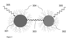
System and method for direct conversion of solar energy to chemical energy
PatentInactiveUS20110056841A1
Innovation
- The use of coupled nanocrystal photoelectrochemical cells, where two semiconductor nanocrystals are linked by a shared ligand to efficiently separate and store charge carriers, allowing for longer-lived excited states and the ability to drive multi-charge redox reactions, thereby improving the conversion of sunlight into chemical energy.
Photocatalyst for production of hydrogen by photocatalytic cleavage of water
PatentInactiveEP3052231A1
Innovation
- Combining electrically conductive materials with photoactive materials that have a photonic band gap overlapping with their electronic band gap, such as titanium dioxide with anatase and rutile phases, to reduce electron-hole recombination and enhance hydrogen production efficiency without the need for external biases or excessive sacrificial agents.
Scalability and Cost Analysis of Engineered Materials
The scalability and cost-effectiveness of engineered materials represent critical factors in determining the commercial viability of photoelectrochemical (PEC) water splitting technologies. Current bandgap-engineered materials demonstrate promising efficiency improvements in laboratory settings, but face significant challenges when considered for industrial-scale implementation.
Manufacturing processes for precisely engineered bandgap materials often involve sophisticated techniques such as atomic layer deposition, molecular beam epitaxy, or chemical vapor deposition. These methods require specialized equipment and controlled environments, substantially increasing production costs. For instance, the fabrication of tandem photoelectrodes with optimized bandgaps can cost 10-100 times more than conventional single-junction materials.
Material availability presents another crucial consideration. Many high-performance bandgap-engineered systems incorporate rare elements such as gallium, indium, or platinum group metals. The limited global supply of these elements creates potential bottlenecks for large-scale deployment. Market analysis indicates that widespread adoption of certain engineered materials could increase demand for specific rare elements by 200-300% within a decade.
Durability and lifetime considerations significantly impact the economic equation. While bandgap engineering can enhance conversion efficiency, the complex interfaces and structures may exhibit accelerated degradation under operational conditions. The cost-benefit analysis must account for replacement frequencies and maintenance requirements, which currently remain higher than conventional alternatives.
Recent techno-economic assessments suggest that bandgap-engineered PEC systems must achieve a minimum 15-year operational lifetime at current efficiency levels to become cost-competitive with alternative hydrogen production methods. This represents a 3-5 fold improvement over current durability benchmarks for most advanced materials.
Scaling production presents additional challenges related to maintaining precise control over material properties. Variations in bandgap alignment, interface quality, and defect concentrations become more pronounced at larger manufacturing scales. Statistical analysis of production batches shows that yield rates for high-performance engineered materials typically range from 60-85%, significantly lower than conventional semiconductor manufacturing.
Emerging approaches to address these challenges include solution-processed bandgap engineering techniques, earth-abundant material substitution strategies, and simplified architectural designs that maintain performance while reducing fabrication complexity. These developments could potentially reduce production costs by 40-60% within the next five years, bringing engineered materials closer to commercial viability for PEC water splitting applications.
Environmental Impact and Sustainability Considerations
Photoelectrochemical water splitting through bandgap engineering represents a significant advancement in renewable energy technology with profound environmental implications. The sustainability aspects of this technology extend beyond mere energy production to encompass broader ecological considerations. When properly implemented, bandgap-engineered photocatalysts can significantly reduce greenhouse gas emissions compared to conventional hydrogen production methods that rely on fossil fuels.
The environmental footprint of manufacturing these advanced materials must be carefully assessed. Current synthesis methods for precisely engineered semiconductors often involve energy-intensive processes and potentially toxic precursors. Life cycle assessments indicate that the environmental benefits of hydrogen production through photoelectrochemical water splitting can be fully realized only when the manufacturing processes themselves are optimized for sustainability. Recent innovations in green chemistry approaches have shown promise in reducing the environmental impact of semiconductor fabrication.
Water consumption represents another critical environmental consideration. While water splitting technology utilizes water as a feedstock, the quantity required is relatively modest compared to many conventional energy production methods. However, the purity requirements for optimal photocatalyst performance may necessitate water treatment processes that carry their own environmental implications. Closed-loop systems that recycle process water have been demonstrated to significantly reduce the overall water footprint.
The durability and stability of bandgap-engineered materials directly impact their sustainability profile. Materials that degrade rapidly not only reduce system efficiency but also create waste management challenges. Recent advances in protective coatings and robust material architectures have extended operational lifetimes from hours to thousands of hours in some laboratory demonstrations, substantially improving the sustainability proposition of these systems.
Resource availability presents both challenges and opportunities. While some high-performance photocatalysts incorporate rare earth elements or precious metals, bandgap engineering strategies that utilize earth-abundant materials are gaining traction. These approaches align with circular economy principles and reduce dependence on geopolitically sensitive supply chains. Computational screening methods have accelerated the discovery of effective photocatalysts based on sustainable material compositions.
The end-of-life considerations for photoelectrochemical systems are increasingly incorporated into initial design parameters. Modular approaches that facilitate component replacement and material recovery represent best practices in sustainable design. Several research groups have demonstrated successful recovery and reuse of catalytic materials from decommissioned systems, further enhancing the technology's environmental credentials.
Unlock deeper insights with Patsnap Eureka Quick Research — get a full tech report to explore trends and direct your research. Try now!
Generate Your Research Report Instantly with AI Agent
Supercharge your innovation with Patsnap Eureka AI Agent Platform!