Nanostructured photoelectrodes for improved water splitting performance.
SEP 4, 202510 MIN READ
Generate Your Research Report Instantly with AI Agent
Patsnap Eureka helps you evaluate technical feasibility & market potential.
Nanostructured Photoelectrodes Background and Objectives
Photoelectrochemical (PEC) water splitting represents a promising approach for sustainable hydrogen production, offering a pathway to convert solar energy directly into chemical energy. The evolution of nanostructured photoelectrodes has been a critical advancement in this field, with research dating back to the pioneering work of Fujishima and Honda in 1972 who demonstrated water splitting using TiO2 electrodes. Since then, the field has witnessed remarkable progress in materials science, nanotechnology, and surface engineering.
The development trajectory of nanostructured photoelectrodes has been characterized by continuous improvements in efficiency, stability, and cost-effectiveness. Early research focused primarily on metal oxide semiconductors such as TiO2, Fe2O3, and WO3. The introduction of nanoscale architectures in the 1990s marked a significant turning point, enabling enhanced light absorption, improved charge separation, and increased surface area for catalytic reactions.
Recent technological trends indicate a shift toward complex hierarchical nanostructures, heterojunction systems, and hybrid organic-inorganic materials. These advancements have been driven by the fundamental understanding that efficient water splitting requires simultaneous optimization of light harvesting, charge carrier dynamics, and catalytic surface reactions.
The emergence of advanced fabrication techniques, including hydrothermal synthesis, electrodeposition, atomic layer deposition, and template-assisted methods, has facilitated precise control over the morphology, composition, and electronic properties of photoelectrodes. This has enabled the creation of sophisticated nanostructures such as nanowires, nanotubes, nanosheets, and three-dimensional networks with tailored properties.
The primary technical objectives for nanostructured photoelectrodes include achieving solar-to-hydrogen conversion efficiencies exceeding 10%, developing materials with long-term stability in aqueous environments, reducing the use of precious metal catalysts, and designing scalable fabrication processes compatible with large-scale production. Additionally, there is a growing emphasis on developing photoelectrodes capable of operating under visible light, which constitutes a significant portion of the solar spectrum.
Theoretical analyses suggest that an ideal photoelectrode system should possess a bandgap of approximately 1.8-2.0 eV to balance light absorption and electrochemical potential requirements. The material should also exhibit appropriate band edge positions, efficient charge transport properties, and catalytic activity for the oxygen evolution reaction (OER) or hydrogen evolution reaction (HER), depending on whether it functions as a photoanode or photocathode.
The ultimate goal of research in this field is to develop integrated PEC systems capable of achieving solar-to-hydrogen efficiencies approaching the theoretical maximum of 30%, while maintaining operational stability for thousands of hours and utilizing earth-abundant materials to ensure economic viability for large-scale deployment.
Market Analysis for Water Splitting Technologies
The global market for water splitting technologies is experiencing significant growth, driven by the increasing demand for clean hydrogen production methods. As of 2023, the market size for water electrolysis technologies has reached approximately $290 million, with projections indicating a compound annual growth rate (CAGR) of 14.5% through 2030. This growth trajectory is primarily fueled by the global push towards decarbonization and the establishment of hydrogen economies in major industrialized nations.
Nanostructured photoelectrodes represent a particularly promising segment within this market, currently accounting for about 8% of the total water splitting technology market. This segment is expected to grow at an accelerated rate of 18.7% annually, outpacing the broader market due to its potential for higher efficiency and lower operational costs.
Geographically, Europe leads the market adoption with approximately 38% market share, followed by North America (27%) and Asia-Pacific (25%). The remaining 10% is distributed across other regions. Within the Asia-Pacific region, Japan and South Korea have demonstrated the most aggressive investment strategies in photoelectrochemical water splitting research and commercialization efforts.
From an end-user perspective, the market can be segmented into industrial hydrogen production (42%), research institutions (31%), renewable energy integration systems (18%), and other applications (9%). The industrial hydrogen production segment is experiencing the fastest growth as industries seek to reduce their carbon footprint through green hydrogen initiatives.
Key market drivers include stringent environmental regulations, declining costs of renewable energy sources, increasing investments in hydrogen infrastructure, and technological advancements in nanomaterials. The European Union's Hydrogen Strategy, which aims to install at least 40GW of renewable hydrogen electrolyzers by 2030, has created a particularly strong market pull for advanced water splitting technologies.
Market barriers include high initial capital costs, efficiency limitations, durability challenges of current photoelectrode materials, and competition from established hydrogen production methods such as steam methane reforming. The levelized cost of hydrogen production using nanostructured photoelectrodes currently ranges from $5.20 to $7.80 per kilogram, compared to $1.50 to $3.50 for conventional methods, presenting a significant commercialization hurdle.
Venture capital investments in startups focusing on nanostructured photoelectrode technologies have reached $420 million in 2022, a 35% increase from the previous year, indicating growing investor confidence in the commercial potential of these technologies despite current technical and economic challenges.
Current Status and Challenges in Photoelectrochemical Water Splitting
Photoelectrochemical (PEC) water splitting represents a promising approach for sustainable hydrogen production using solar energy. Currently, the field has achieved significant milestones, with laboratory-scale devices demonstrating solar-to-hydrogen (STH) conversion efficiencies ranging from 10% to 19% under controlled conditions. However, these achievements remain far from commercial viability, which requires efficiencies exceeding 20% alongside decade-long stability.
The primary technical challenges in PEC water splitting revolve around three critical aspects: efficiency, stability, and cost. Regarding efficiency, most nanostructured photoelectrodes still suffer from high recombination rates of photogenerated charge carriers, limiting quantum yields. The band gap engineering of semiconductor materials presents another challenge, as optimal materials must balance light absorption breadth with sufficient electrochemical potential for water splitting.
Stability issues persist as a major obstacle, with many high-performance materials experiencing rapid degradation in aqueous environments. Silicon-based photoelectrodes, despite their excellent light absorption properties, suffer from photocorrosion, while metal oxide semiconductors often demonstrate poor charge transport characteristics. Protection strategies using conformal coatings have shown promise but frequently compromise efficiency or increase system complexity.
From a geographical perspective, research leadership in PEC water splitting is distributed across North America, Europe, and East Asia. The United States maintains strong fundamental research programs through the Department of Energy and university consortia, while Japan and South Korea focus on materials innovation and device integration. European research centers, particularly in Germany and Switzerland, lead in systems engineering and scale-up methodologies.
Cost factors present significant barriers to commercialization. Current high-efficiency systems rely on precious metal catalysts like platinum and iridium, which are prohibitively expensive for large-scale deployment. Additionally, manufacturing processes for nanostructured photoelectrodes often involve energy-intensive or complex fabrication steps that are difficult to scale economically.
Recent technological constraints also include the integration challenges between different components of PEC systems. The interface engineering between photoabsorbers, catalysts, and protective layers remains problematic, with charge transfer losses occurring at these critical junctions. Furthermore, the development of standardized testing protocols and benchmarking methods has been inconsistent, making direct comparisons between different research approaches difficult.
The field is currently transitioning from proof-of-concept demonstrations to practical engineering solutions, with increasing focus on tandem photoelectrode architectures that can more effectively utilize the solar spectrum. However, bridging the gap between laboratory performance and commercial requirements necessitates breakthrough innovations in materials science, interface engineering, and manufacturing processes.
State-of-the-Art Nanostructured Photoelectrode Solutions
01 Metal oxide nanostructures for enhanced photoelectrochemical water splitting
Metal oxide nanostructures, particularly titanium dioxide (TiO2), hematite (Fe2O3), and tungsten trioxide (WO3), can be engineered to enhance photoelectrochemical water splitting performance. These materials offer advantages such as high surface area, efficient charge separation, and improved light absorption. By controlling the morphology, crystallinity, and doping of these metal oxide nanostructures, the photoelectrochemical efficiency for hydrogen production can be significantly improved.- Metal oxide nanostructures for enhanced photoelectrochemical water splitting: Metal oxide nanostructures, such as titanium dioxide, hematite, and tungsten oxide, can be engineered to enhance photoelectrochemical water splitting performance. These materials offer advantages including high surface area, improved light absorption, and efficient charge separation. By controlling the morphology, crystallinity, and doping of these nanostructures, the water splitting efficiency can be significantly improved, leading to higher hydrogen production rates.
- Doping and heterostructure engineering for improved charge carrier dynamics: Doping photoelectrodes with various elements and creating heterostructures can significantly enhance water splitting performance by improving charge carrier generation, separation, and transport. These modifications reduce recombination rates and extend the light absorption range into the visible spectrum. Strategic combinations of materials create beneficial band alignments that facilitate efficient electron-hole separation, resulting in higher photocurrent densities and improved solar-to-hydrogen conversion efficiencies.
- One-dimensional nanostructures for directional charge transport: One-dimensional nanostructures such as nanorods, nanowires, and nanotubes offer directional pathways for charge transport in photoelectrochemical water splitting systems. These structures minimize charge recombination by providing direct routes for electrons and holes to reach their respective reaction sites. The high aspect ratio of these nanostructures also increases the electrode-electrolyte interface area, enhancing catalytic activity while maintaining good mechanical stability and light absorption properties.
- Surface modification and co-catalyst integration: Surface modification techniques and co-catalyst integration can significantly enhance the performance of nanostructured photoelectrodes for water splitting. Strategies include depositing noble metal nanoparticles, transition metal compounds, or carbon-based materials on the photoelectrode surface. These modifications reduce the activation energy for water oxidation or hydrogen evolution reactions, passivate surface defects, and improve the stability of photoelectrodes in aqueous environments, resulting in higher solar-to-hydrogen conversion efficiencies.
- Hierarchical and composite nanostructures for multifunctional performance: Hierarchical and composite nanostructures combine multiple materials and architectural designs to address various limitations in photoelectrochemical water splitting. These complex structures simultaneously optimize light harvesting, charge separation, catalytic activity, and stability. By integrating different functional components at various scales, these photoelectrodes can achieve synergistic effects that significantly enhance overall water splitting performance compared to single-component systems, making them promising candidates for practical solar hydrogen production.
02 Doping and heterostructure formation for improved charge separation
Doping photoelectrode materials with metal or non-metal elements and creating heterostructures can significantly enhance water splitting performance. These modifications improve charge carrier separation, reduce recombination rates, and extend light absorption into the visible spectrum. Heterostructures formed between different semiconductors create beneficial band alignments that facilitate efficient electron-hole separation and transfer, leading to higher photocurrent densities and improved solar-to-hydrogen conversion efficiencies.Expand Specific Solutions03 Novel fabrication methods for nanostructured photoelectrodes
Advanced fabrication techniques such as hydrothermal synthesis, electrodeposition, sol-gel methods, and template-assisted growth enable precise control over the morphology and composition of nanostructured photoelectrodes. These methods allow for the creation of various nanostructures including nanorods, nanotubes, nanosheets, and hierarchical structures with optimized dimensions and orientations. Such tailored architectures facilitate efficient light harvesting, charge transport, and catalytic reactions at the semiconductor-electrolyte interface.Expand Specific Solutions04 Surface modification and co-catalyst integration
Surface modification of photoelectrodes with co-catalysts such as platinum, ruthenium oxide, or cobalt phosphate can significantly enhance water splitting performance. These co-catalysts reduce the activation energy for water oxidation or hydrogen evolution reactions, improving reaction kinetics. Additionally, surface passivation layers can reduce surface recombination and enhance stability in aqueous environments. Strategic placement of co-catalysts on specific facets of nanostructured photoelectrodes can further optimize charge transfer and catalytic efficiency.Expand Specific Solutions05 Carbon-based and composite photoelectrode materials
Carbon-based materials such as graphene, carbon nanotubes, and carbon quantum dots can be incorporated into photoelectrode structures to enhance conductivity and charge transport properties. These carbon-based components can form composites with traditional semiconductor materials, creating synergistic effects that improve light absorption, charge separation, and catalytic activity. Additionally, carbon-based materials can serve as supports for dispersing catalytic nanoparticles, further enhancing the water splitting performance of photoelectrodes.Expand Specific Solutions
Leading Research Groups and Companies in Water Splitting
The nanostructured photoelectrodes for water splitting market is currently in a growth phase, with increasing research activity across academic and industrial sectors. The market size is expanding as clean hydrogen production becomes central to renewable energy strategies, estimated to reach several billion dollars by 2030. Technologically, the field shows moderate maturity with significant ongoing innovation. Leading research institutions like King Abdullah University of Science & Technology, University of Tokyo, and California Institute of Technology are advancing fundamental science, while companies such as FUJIFILM Corp., S-Oil Corp., and EDAC Labs are focusing on commercialization pathways. The competitive landscape features strong collaboration between academic institutions and industrial partners, with Asian and Middle Eastern players showing particular strength in photoelectrode development for solar-driven water splitting applications.
Ulsan National Institute of Science & Technology
Technical Solution: UNIST has developed innovative nanostructured photoelectrodes based on earth-abundant materials for cost-effective water splitting. Their approach centers on hierarchical titanium dioxide (TiO2) nanostructures with controlled oxygen vacancy concentrations to enhance visible light absorption. UNIST researchers have pioneered a unique hydrothermal synthesis method that creates highly ordered, vertically aligned TiO2 nanotube arrays with precisely controlled dimensions (20-100 nm diameter, 5-20 μm length) and crystallinity. These photoelectrodes are further enhanced through strategic nitrogen doping and surface modification with plasmonic nanoparticles, extending light absorption into the visible range. Their most recent innovation involves a core-shell nanostructure design where an ultrathin (2-5 nm) layer of amorphous TiO2 encapsulates a crystalline core, creating beneficial band bending at interfaces that significantly improves charge separation efficiency and reduces recombination losses.
Strengths: Excellent scalability using earth-abundant materials; remarkable stability in various pH conditions; cost-effective fabrication methods suitable for large-scale production. Weaknesses: Lower overall efficiency compared to noble metal-based systems; limited performance in the near-infrared region of the solar spectrum.
University of Tokyo
Technical Solution: The University of Tokyo has developed sophisticated nanostructured photoelectrodes based on innovative metal oxide semiconductors for efficient solar water splitting. Their approach focuses on creating complex oxide heterostructures with precisely controlled interfaces at the nanoscale. Their researchers have pioneered advanced pulsed laser deposition techniques to create epitaxial thin films of materials like SrTiO3, Fe2O3, and BiVO4 with atomically flat surfaces and controlled defect concentrations. A key innovation is their development of gradient-doped hematite (α-Fe2O3) nanorod arrays that feature strategic elemental doping (Ti, Sn, Zr) with concentration gradients from core to surface, optimizing both bulk conductivity and surface catalytic activity. These photoelectrodes demonstrate remarkable charge separation efficiency through built-in electric fields at engineered heterojunctions. Their most recent breakthrough involves plasmonic-enhanced photoelectrodes that utilize gold nanoislands to create localized electromagnetic field enhancement, significantly boosting light absorption and charge generation in the visible spectrum.
Strengths: Exceptional control over material interfaces and crystallinity; superior understanding of fundamental charge transfer mechanisms; excellent stability under operating conditions. Weaknesses: Relatively complex and expensive fabrication processes; some designs rely on noble metals that may limit large-scale economic viability.
Key Patents and Scientific Breakthroughs in Photoelectrode Design
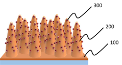
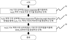
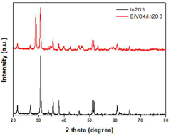
Photoelectrode comprising bismuth vanadate/indium oxide heterogeneous nanorods and manufacturing method thereof
PatentActiveKR1020210144385A
Innovation
- A photoelectrode comprising a bismuth vanadate/indium oxide heterojunction nanorod structure is formed by electrodepositing bismuth vanadate on an indium oxide nanorod, utilizing a glancing angle deposition and pulse-based electrodeposition methods to create a Type II band structure, enhancing light absorption, charge separation, and surface area.

Scalability and Manufacturing Considerations
The transition from laboratory-scale demonstrations to industrial production represents a critical challenge for nanostructured photoelectrodes in water splitting applications. Current fabrication methods such as hydrothermal synthesis, sol-gel processing, and electrodeposition show promising results at small scales but face significant hurdles when considered for mass production. These challenges include maintaining structural uniformity, ensuring consistent performance, and managing production costs at larger scales.
Material selection plays a crucial role in scalability considerations. While certain nanomaterials demonstrate excellent photoelectrochemical properties, their commercial viability depends on abundance, extraction costs, and processing requirements. Rare earth elements and precious metals, despite their superior performance, present sustainability concerns for large-scale deployment. Alternative approaches using earth-abundant materials like iron oxide, zinc oxide, and carbon-based structures are gaining attention as scalable alternatives, albeit with performance trade-offs.
Manufacturing techniques require substantial adaptation for industrial implementation. Roll-to-roll processing shows promise for continuous production of thin-film photoelectrodes, potentially reducing production costs by 30-40% compared to batch processes. Spray pyrolysis and inkjet printing technologies offer additional pathways for scaled manufacturing, with recent advancements improving deposition uniformity across large surface areas. These techniques must balance precision with throughput to be economically viable.
Quality control represents another significant challenge in scaled production. Nanoscale features that determine performance characteristics require sophisticated monitoring systems during manufacturing. Advanced characterization techniques such as in-line spectroscopic ellipsometry and automated electrochemical testing are being developed to ensure consistent performance across production batches. Statistical process control methodologies adapted for nanomaterial production show promising results in maintaining quality standards.
Economic considerations ultimately determine commercial feasibility. Current cost analyses indicate that nanostructured photoelectrode production remains 3-5 times more expensive than conventional alternatives. However, learning curve effects and economies of scale could reduce this gap significantly. Recent modeling suggests that with optimized manufacturing processes and increased production volumes, cost parity might be achievable within 5-7 years, particularly if coupled with improvements in device longevity and efficiency.
Environmental and safety considerations must also be addressed in manufacturing scale-up. Nanoparticle handling presents unique workplace safety challenges, requiring specialized containment systems and monitoring protocols. Sustainable manufacturing approaches that minimize waste generation and energy consumption are increasingly being integrated into production planning, with closed-loop solvent recovery systems demonstrating both environmental and economic benefits in pilot-scale operations.
Environmental Impact and Sustainability Assessment
The environmental impact of nanostructured photoelectrodes for water splitting extends far beyond their immediate application in hydrogen production. These advanced materials offer significant potential for reducing global carbon emissions by enabling efficient conversion of solar energy into clean hydrogen fuel. When implemented at scale, this technology could substantially decrease dependence on fossil fuels for hydrogen production, which currently accounts for approximately 830 million tonnes of CO2 emissions annually.
The sustainability profile of nanostructured photoelectrodes must be evaluated through comprehensive life cycle assessment (LCA). Current analyses indicate that while the manufacturing processes for these specialized materials can be energy-intensive, the net environmental benefit over the operational lifetime typically outweighs the initial carbon footprint. The energy payback period for most photoelectrochemical systems ranges from 1-3 years, depending on material composition and fabrication methods.
Material selection presents critical sustainability considerations. Many high-performance photoelectrodes incorporate rare earth elements or precious metals like platinum and iridium as catalysts. The extraction and processing of these materials carry significant environmental burdens, including habitat destruction, water pollution, and high energy consumption. Research into earth-abundant alternatives such as nickel-iron oxides and cobalt phosphates shows promising directions for reducing resource intensity without compromising performance.
Water consumption and quality impacts must also be carefully managed. While water splitting systems utilize water as a feedstock, the quantity required is minimal compared to many industrial processes. However, the purity requirements can necessitate energy-intensive water treatment processes. Closed-loop systems that recycle process water represent an important advancement for reducing the overall water footprint.
End-of-life considerations for nanostructured materials present unique challenges. The nanoscale dimensions of these materials can complicate recycling efforts and raise concerns about potential environmental release. Developing effective recovery and recycling protocols for spent photoelectrodes will be essential for ensuring true sustainability. Current research indicates that up to 85% of precious metal catalysts can be recovered through appropriate recycling techniques.
The scalability of environmentally responsible manufacturing processes remains a significant hurdle. Laboratory-scale fabrication methods often employ hazardous chemicals and energy-intensive processes that would pose substantial environmental risks if directly scaled to industrial production. Transitioning to greener synthesis routes, such as hydrothermal methods and electrodeposition techniques, represents a crucial step toward truly sustainable implementation.
Unlock deeper insights with Patsnap Eureka Quick Research — get a full tech report to explore trends and direct your research. Try now!
Generate Your Research Report Instantly with AI Agent
Supercharge your innovation with Patsnap Eureka AI Agent Platform!