How to Control Grain Boundary Effects in Polycrystalline Skutterudite Materials
AUG 27, 20259 MIN READ
Generate Your Research Report Instantly with AI Agent
Patsnap Eureka helps you evaluate technical feasibility & market potential.
Skutterudite Materials Background and Research Objectives
Skutterudite compounds, first discovered in the mineral deposits of Skutterud, Norway in the 19th century, represent a significant class of thermoelectric materials with the general formula MX3 (where M typically represents Co, Rh, or Ir, and X represents P, As, or Sb). These materials have garnered substantial research interest due to their intrinsic "phonon-glass electron-crystal" (PGEC) characteristics, which enable them to simultaneously possess low thermal conductivity and high electrical conductivity—properties crucial for efficient thermoelectric energy conversion.
The evolution of skutterudite research has progressed through several distinct phases. Initial investigations in the 1950s and 1960s focused primarily on understanding the basic crystallographic structure and electronic properties. The 1990s marked a renaissance in skutterudite research when Slack proposed the PGEC concept, suggesting that the large voids in the skutterudite structure could be filled with loosely bound atoms ("rattlers") to scatter phonons and reduce thermal conductivity without significantly affecting electronic transport.
Recent technological advances have shifted focus toward polycrystalline skutterudite materials, which offer practical advantages in terms of manufacturing scalability and cost-effectiveness compared to single crystals. However, this transition has introduced significant challenges related to grain boundary effects, which can substantially impact thermoelectric performance through electron and phonon scattering mechanisms.
The primary objective of this technical research is to develop comprehensive strategies for controlling grain boundary effects in polycrystalline skutterudite materials to optimize their thermoelectric performance. Specifically, we aim to understand the fundamental mechanisms governing grain boundary formation, characterize their structural and compositional features, and develop innovative processing techniques to manipulate these interfaces advantageously.
Secondary objectives include establishing quantitative relationships between grain boundary characteristics and thermoelectric properties, developing predictive models for optimizing grain boundary engineering, and exploring novel doping and alloying strategies that can selectively modify grain boundary regions without compromising bulk properties.
The technological trajectory suggests that mastering grain boundary effects could potentially increase the dimensionless figure of merit (ZT) of skutterudite materials by 30-50%, which would represent a significant advancement toward commercial viability for medium-temperature (400-600°C) thermoelectric applications in waste heat recovery systems, automotive thermoelectric generators, and distributed power generation.
This research aligns with broader global initiatives to improve energy efficiency and reduce carbon emissions through advanced materials technology, positioning skutterudite materials as key components in the sustainable energy landscape of the future.
Market Analysis for Thermoelectric Materials and Applications
The global thermoelectric materials market is experiencing significant growth, driven by increasing demand for energy-efficient technologies and waste heat recovery systems. Currently valued at approximately $51 billion in 2023, the market is projected to reach $79 billion by 2028, representing a compound annual growth rate (CAGR) of 9.2%. This growth trajectory is supported by expanding applications across automotive, industrial manufacturing, consumer electronics, and aerospace sectors.
Skutterudite-based thermoelectric materials represent a promising segment within this market due to their superior performance characteristics in mid-to-high temperature ranges (400-700°C). These materials offer a compelling combination of high thermoelectric figure of merit (ZT values reaching 1.7), relatively low toxicity compared to lead-based alternatives, and potential for cost-effective manufacturing at scale.
The automotive sector currently constitutes the largest application market for thermoelectric materials, accounting for 38% of total demand. Waste heat recovery systems in vehicles can improve fuel efficiency by 3-5%, creating significant value in a market increasingly focused on emissions reduction. Major automotive manufacturers including BMW, Toyota, and Ford have active research programs exploring skutterudite integration in exhaust heat recovery systems.
Industrial waste heat recovery represents another substantial market opportunity, with global industrial processes wasting approximately 20-50% of consumed energy as heat. The International Energy Agency estimates that industrial waste heat recovery could reduce global industrial energy consumption by up to 10%, creating a market potential of $14 billion for thermoelectric solutions by 2026.
Consumer electronics applications are growing rapidly at 12.3% CAGR, driven by demand for self-powered IoT devices and wearable technology. Miniaturized thermoelectric generators based on advanced materials like skutterudites could enable energy harvesting capabilities in next-generation consumer products.
Regionally, Asia-Pacific dominates the market with 42% share, followed by North America (28%) and Europe (23%). China has emerged as both the largest consumer and producer of thermoelectric materials, with substantial government investment in research and manufacturing capabilities.
Market challenges include competition from alternative waste heat recovery technologies (Organic Rankine Cycle systems, thermophotovoltaics), material cost considerations, and manufacturing scalability issues. However, ongoing advances in controlling grain boundary effects in polycrystalline skutterudites could significantly improve performance-to-cost ratios, potentially expanding market penetration across all application segments.
Current Challenges in Polycrystalline Skutterudite Grain Boundary Control
Polycrystalline skutterudite materials have emerged as promising candidates for thermoelectric applications due to their intrinsic "phonon glass-electron crystal" characteristics. However, controlling grain boundary effects remains one of the most significant challenges in optimizing their performance. The grain boundaries in these materials act as scattering centers for both phonons and charge carriers, creating a complex trade-off between thermal and electrical transport properties.
The primary challenge lies in the inherent contradiction between thermal and electrical conductivity optimization. While increased grain boundary density can effectively reduce lattice thermal conductivity through phonon scattering, it simultaneously impedes electron transport, resulting in decreased electrical conductivity. This fundamental conflict necessitates sophisticated engineering approaches to selectively influence phonon and electron transport at grain boundaries.
Another significant obstacle is the chemical and structural instability at grain boundaries in skutterudites. The complex crystal structure of skutterudites, with its characteristic pnictogen rings and voids, becomes particularly vulnerable at grain interfaces. These regions often exhibit phase segregation, impurity accumulation, and oxidation, especially during high-temperature operation cycles typical in thermoelectric applications.
Precise characterization of grain boundaries presents additional technical difficulties. Current analytical techniques struggle to provide comprehensive three-dimensional information about grain boundary structure, composition, and electronic states in skutterudites. This limitation hinders the development of targeted strategies for grain boundary engineering.
The reproducible synthesis of skutterudites with controlled grain size distribution and boundary characteristics remains challenging. Conventional powder metallurgy approaches often result in heterogeneous microstructures with unpredictable grain boundary properties. Advanced processing techniques like spark plasma sintering offer improved control but introduce additional complexities related to rapid heating rates and non-equilibrium conditions.
Furthermore, the filling of voids in skutterudites with guest atoms—a common strategy to reduce thermal conductivity—introduces additional complexity to grain boundary management. These filler atoms often segregate preferentially at grain boundaries, altering local electronic structure and potentially creating undesired secondary phases.
Computational modeling of grain boundary effects in skutterudites is hindered by the complex crystal structure and the multiscale nature of the relevant phenomena. Current models struggle to accurately predict how specific grain boundary characteristics will influence macroscopic thermoelectric properties, limiting the effectiveness of theory-guided design approaches.
Current Methodologies for Grain Boundary Modification
01 Grain boundary engineering in skutterudite materials
Grain boundary engineering techniques are applied to skutterudite materials to control and modify the microstructure of polycrystalline skutterudites. These techniques involve manipulating the grain size, orientation, and boundary characteristics to enhance thermoelectric performance. By controlling the grain boundary density and structure, thermal conductivity can be reduced while maintaining good electrical properties, leading to improved figure of merit (ZT) values in skutterudite-based thermoelectric materials.- Grain boundary engineering in skutterudite materials: Grain boundary engineering techniques are applied to skutterudite materials to control and optimize the microstructure. By manipulating the grain boundaries, the thermal and electrical properties of polycrystalline skutterudites can be enhanced. These techniques include controlling grain size, orientation, and boundary characteristics to reduce thermal conductivity while maintaining good electrical conductivity, which is crucial for thermoelectric applications.
- Doping effects on grain boundaries in skutterudites: Introducing dopants at grain boundaries in polycrystalline skutterudite materials can significantly alter their thermoelectric performance. Dopants can segregate at grain boundaries, creating energy barriers that scatter phonons more effectively than electrons, thereby reducing thermal conductivity while preserving electrical conductivity. Various elements can be used as dopants to tailor the grain boundary properties for specific applications.
- Nanostructuring approaches for grain boundary modification: Nanostructuring techniques are employed to modify grain boundaries in skutterudite materials. These approaches include creating nanoinclusions, precipitates, or secondary phases at grain boundaries to enhance phonon scattering. The controlled introduction of nanoscale features at grain boundaries can significantly reduce thermal conductivity through increased phonon scattering while maintaining electrical transport properties.
- Processing methods affecting grain boundary characteristics: Various processing methods significantly impact the grain boundary characteristics of polycrystalline skutterudite materials. Techniques such as hot pressing, spark plasma sintering, and annealing treatments can control grain growth, boundary formation, and interfacial properties. The processing conditions directly influence the microstructure development, which in turn affects the thermal and electrical transport across grain boundaries.
- Characterization and modeling of grain boundary effects: Advanced characterization techniques and theoretical modeling are used to understand grain boundary effects in skutterudite materials. Electron microscopy, spectroscopy, and computational methods help analyze the structure and composition of grain boundaries and their impact on carrier transport. These studies provide insights into the fundamental mechanisms of how grain boundaries influence thermal and electrical properties, guiding the design of high-performance thermoelectric skutterudites.
02 Nanostructuring effects on skutterudite grain boundaries
Nanostructuring approaches are employed to modify grain boundaries in skutterudite materials, creating nanoscale features that enhance phonon scattering at interfaces. These approaches include the incorporation of nanoinclusions, nanoparticles, or nanoprecipitates at grain boundaries, which effectively scatter phonons while minimally affecting electron transport. The controlled introduction of nanoscale features at grain boundaries significantly reduces lattice thermal conductivity in polycrystalline skutterudites, improving their thermoelectric performance.Expand Specific Solutions03 Doping and filling effects on skutterudite grain boundaries
Various doping and filling strategies are employed to modify the grain boundary properties of skutterudite materials. Introducing specific elements into the skutterudite structure or at grain boundaries can alter the electronic structure, carrier concentration, and phonon transport across boundaries. Filled skutterudites with optimized grain boundary composition demonstrate enhanced thermoelectric performance due to the combined effects of reduced thermal conductivity at boundaries and improved electrical transport properties.Expand Specific Solutions04 Processing techniques for grain boundary control in skutterudites
Specialized processing techniques are developed to control grain boundary formation and characteristics in polycrystalline skutterudite materials. These techniques include specific sintering methods, hot pressing parameters, spark plasma sintering, and post-processing treatments that influence grain growth, boundary formation, and interfacial properties. Optimized processing conditions lead to favorable grain boundary structures that enhance phonon scattering while maintaining good electrical conductivity across grain boundaries.Expand Specific Solutions05 Characterization and modeling of grain boundary effects in skutterudites
Advanced characterization techniques and theoretical modeling approaches are employed to understand grain boundary effects in polycrystalline skutterudite materials. These include electron microscopy, spectroscopy, and computational methods to analyze grain boundary structure, composition, and transport properties. The insights gained from these studies enable the development of predictive models for grain boundary engineering, leading to optimized skutterudite materials with enhanced thermoelectric performance through controlled grain boundary effects.Expand Specific Solutions
Leading Research Groups and Companies in Skutterudite Development
The control of grain boundary effects in polycrystalline skutterudite materials represents a critical technological challenge in the evolving thermoelectric materials landscape. The market is currently in a growth phase, with an estimated global thermoelectric materials market exceeding $600 million and projected to expand significantly due to increasing demand for waste heat recovery systems. Leading research institutions like MIT, Tohoku University, and Rensselaer Polytechnic Institute are advancing fundamental understanding, while companies including Samsung Electronics, Hitachi, and Mitsubishi Materials are developing commercial applications. The technology remains in mid-maturity stage, with significant breakthroughs in grain boundary engineering coming from collaborative efforts between academic institutions and industrial players like GLOBALFOUNDRIES and Infineon Technologies, who are exploring integration with semiconductor manufacturing processes.
Tohoku University
Technical Solution: Tohoku University has developed an innovative approach to control grain boundary effects in polycrystalline skutterudite materials through a combination of high-pressure synthesis and microstructural engineering. Their technique involves precise control of the sintering process using spark plasma sintering (SPS) under optimized pressure conditions (50-100 MPa) and temperatures (600-700°C), which significantly reduces grain boundary resistance. They've pioneered the use of nanoscale precipitates at grain boundaries to create beneficial phonon scattering centers while maintaining electron transport. Their research demonstrates that controlled introduction of specific dopants (such as rare earth elements Nd, Ce, and La) can effectively modify grain boundary characteristics, resulting in enhanced thermoelectric performance with ZT values exceeding 1.5 at moderate temperatures. The university has also developed post-processing annealing protocols that promote grain boundary healing and reduce detrimental carrier scattering.
Strengths: Advanced high-pressure synthesis capabilities allowing precise microstructural control; extensive expertise in rare earth element doping strategies; comprehensive characterization facilities for nanoscale analysis of grain boundaries. Weaknesses: Their techniques require specialized high-pressure equipment that may limit industrial scalability; some of their approaches involve costly rare earth elements that could impact commercial viability.
Mitsubishi Materials Corp.
Technical Solution: Mitsubishi Materials has developed a proprietary manufacturing process for high-performance polycrystalline skutterudite materials with controlled grain boundary effects. Their approach combines mechanical alloying with hot pressing techniques under precisely controlled atmospheres to manipulate grain boundary composition and structure. The company employs a multi-stage sintering process that includes an initial low-temperature consolidation phase (350-450°C) followed by controlled grain growth at higher temperatures (600-700°C). This creates optimized grain boundary networks that minimize carrier scattering while enhancing phonon scattering for improved thermoelectric performance. Mitsubishi has also pioneered the use of nano-inclusions (5-20 nm) of secondary phases at grain boundaries, which serve as effective phonon scattering centers without significantly impeding electron transport. Their materials demonstrate thermal conductivity reductions of up to 30% compared to conventional skutterudites while maintaining electrical conductivity, resulting in ZT values approaching 1.7 at operating temperatures.
Strengths: Established industrial-scale production capabilities; proprietary grain boundary engineering techniques applicable to mass production; strong integration with existing thermoelectric device manufacturing. Weaknesses: Their approach may be more focused on production efficiency than achieving theoretical maximum performance; some of their techniques are optimized for specific skutterudite compositions and may not be universally applicable.
Key Patents and Literature on Skutterudite Grain Boundary Control
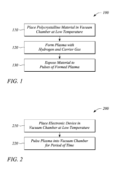
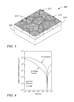
Grain boundary passivation of polycrystalline materials
PatentActiveUS10490689B1
Innovation
- A low-temperature, controlled plasma passivation method using hydrogen atoms is applied to incorporate hydrogen into grain boundaries of polycrystalline semiconductor materials, reducing dark current density and improving performance metrics without damaging underlying circuitry or structures.
Material Characterization Techniques for Grain Boundary Analysis
Advanced characterization techniques are essential for understanding and controlling grain boundary effects in polycrystalline skutterudite materials. Electron microscopy techniques, particularly Transmission Electron Microscopy (TEM) and Scanning Electron Microscopy (SEM), provide direct visualization of grain boundaries at nanometer and micrometer scales respectively. TEM offers atomic-level resolution crucial for observing grain boundary structure, while SEM with Electron Backscatter Diffraction (EBSD) mapping enables comprehensive analysis of grain orientation relationships and boundary distributions across larger sample areas.
X-ray diffraction (XRD) techniques, including high-resolution XRD and small-angle X-ray scattering (SAXS), provide statistical information about crystallite size, strain, and texture in skutterudite materials. These non-destructive methods can track grain boundary evolution during thermal processing or mechanical deformation, offering insights into boundary formation mechanisms.
Spectroscopic techniques such as Energy Dispersive X-ray Spectroscopy (EDS) and Electron Energy Loss Spectroscopy (EELS) are invaluable for chemical analysis at grain boundaries. These methods can detect elemental segregation and second-phase precipitation at boundaries, which significantly influence thermal and electrical transport properties in skutterudites. Atom Probe Tomography (APT) further extends this capability by providing three-dimensional atomic-scale compositional mapping of grain boundary regions.
Thermal and electrical property measurement techniques specifically designed for boundary analysis include thermal conductivity mapping, which can isolate the contribution of grain boundaries to overall thermal resistance. Similarly, micro-four-point probe measurements can quantify electrical transport across individual grain boundaries, providing direct correlation between boundary structure and functional properties.
Advanced computational techniques complement experimental methods through multi-scale modeling approaches. Density Functional Theory (DFT) calculations can predict energetically favorable boundary configurations, while Molecular Dynamics (MD) simulations model thermal transport across boundaries. These computational tools help interpret experimental data and guide experimental design for boundary engineering.
In-situ characterization represents the frontier of grain boundary analysis, allowing real-time observation of boundary behavior under thermal gradients, electrical fields, or mechanical stress. These techniques are particularly valuable for skutterudites, where understanding dynamic boundary processes during operation is crucial for optimizing thermoelectric performance and stability.
Environmental Impact and Sustainability of Skutterudite Processing
The environmental footprint of skutterudite materials processing presents significant sustainability challenges that must be addressed as these thermoelectric materials gain prominence in waste heat recovery applications. Traditional synthesis methods for skutterudite compounds often involve energy-intensive processes requiring high temperatures (600-950°C) and extended reaction times, resulting in substantial carbon emissions. The extraction of constituent elements—particularly cobalt, antimony, and rare earth dopants—raises additional environmental concerns related to mining impacts, habitat disruption, and potential toxic waste generation.
Processing polycrystalline skutterudites typically involves multiple energy-intensive steps including melting, annealing, ball milling, and hot pressing or spark plasma sintering. These processes consume considerable energy and may release harmful particulates and volatile compounds, particularly from antimony-containing precursors which pose toxicity risks. The grain boundary engineering techniques employed to control thermoelectric performance often require additional chemical treatments or processing steps that further increase environmental burden.
Water usage represents another critical environmental consideration, as wet chemical methods and cooling systems in high-temperature processing equipment demand substantial water resources. The chemical waste streams generated during synthesis and post-processing treatments may contain heavy metals and toxic compounds requiring specialized disposal protocols to prevent environmental contamination.
Recent sustainability initiatives have focused on developing greener synthesis routes for skutterudite materials. Mechanochemical approaches using room-temperature ball milling have demonstrated reduced energy requirements compared to conventional high-temperature methods. Microwave-assisted synthesis has emerged as another promising alternative, potentially reducing processing times by 70-80% and energy consumption by up to 50% compared to conventional heating methods.
Recycling and recovery strategies for end-of-life skutterudite devices remain underdeveloped, presenting opportunities for circular economy approaches. The complex composition of these materials, including multiple elements and dopants, complicates recycling efforts but also increases the economic incentive for recovery of valuable constituents. Life cycle assessment studies indicate that despite energy-intensive production, skutterudite thermoelectric generators can achieve net environmental benefits through their operational lifetime when deployed in waste heat recovery applications.
Regulatory frameworks governing skutterudite processing vary significantly across regions, with stricter environmental controls in Europe and North America compared to some developing economies. This regulatory disparity creates challenges for establishing globally sustainable supply chains and manufacturing practices for skutterudite-based technologies.
Unlock deeper insights with Patsnap Eureka Quick Research — get a full tech report to explore trends and direct your research. Try now!
Generate Your Research Report Instantly with AI Agent
Supercharge your innovation with Patsnap Eureka AI Agent Platform!