Skutterudite Thin Films: Deposition Techniques and Thermoelectric Characterization
AUG 27, 202510 MIN READ
Generate Your Research Report Instantly with AI Agent
Patsnap Eureka helps you evaluate technical feasibility & market potential.
Skutterudite Thin Film Technology Background and Objectives
Skutterudite compounds, first discovered in the mid-19th century in Skutterud, Norway, have emerged as promising thermoelectric materials over the past three decades. These cobalt arsenide-based materials (CoAs3) and their filled variants have attracted significant attention due to their excellent thermoelectric properties, particularly at mid-to-high temperatures (400-800K). The evolution of skutterudite research has progressed from bulk materials to thin films, representing a critical advancement in thermoelectric technology miniaturization and integration capabilities.
The development trajectory of skutterudite technology has been marked by several key milestones. Initial research in the 1990s focused primarily on understanding the fundamental properties of bulk skutterudites. By the early 2000s, researchers began exploring "filled skutterudites" where guest atoms are inserted into the crystal structure to reduce thermal conductivity while maintaining electrical conductivity. The transition to thin film research began gaining momentum around 2010, driven by the need for device miniaturization and integration with microelectronic systems.
Thin film skutterudites represent a technological frontier that combines the excellent thermoelectric properties of these materials with the advantages of thin film geometry, including reduced material usage, flexibility in device design, and compatibility with semiconductor processing techniques. This convergence creates opportunities for novel micro-scale thermoelectric generators and cooling devices that were previously unattainable with bulk materials.
The primary technical objectives in skutterudite thin film research center around three critical areas: deposition technique optimization, thermoelectric performance enhancement, and long-term stability improvement. Deposition techniques including sputtering, pulsed laser deposition (PLD), flash evaporation, and molecular beam epitaxy (MBE) are being explored to achieve high-quality, stoichiometrically precise films with controlled microstructure. Simultaneously, researchers aim to maximize the thermoelectric figure of merit (ZT) through compositional tuning, nanostructuring, and interface engineering.
Current research trends indicate growing interest in multi-layered skutterudite thin films, where alternating layers of different compositions create quantum well effects that enhance thermoelectric performance. Additionally, the integration of skutterudite thin films with flexible substrates is emerging as a promising direction for wearable thermoelectric devices. The field is also witnessing increased efforts in computational modeling to predict optimal compositions and structures before experimental validation.
The ultimate goal of skutterudite thin film technology development is to achieve commercially viable thermoelectric devices for waste heat recovery, spot cooling in electronics, and self-powered sensors. This requires addressing the current limitations in deposition scalability, film adhesion, and performance consistency while maintaining competitive production costs compared to alternative thermoelectric technologies.
Market Analysis for Thermoelectric Materials and Applications
The global thermoelectric materials market is experiencing significant growth, valued at approximately $51.6 billion in 2022 and projected to reach $79.7 billion by 2028, representing a compound annual growth rate (CAGR) of 7.5%. This expansion is primarily driven by increasing demand for energy-efficient solutions across various industries, particularly automotive, aerospace, and consumer electronics.
Skutterudite-based thermoelectric materials, including thin films, are gaining substantial market traction due to their superior performance characteristics compared to traditional thermoelectric materials. These materials offer higher ZT values (figure of merit for thermoelectric efficiency) at mid-to-high temperature ranges, making them particularly valuable for waste heat recovery applications in industrial processes and automotive exhaust systems.
The automotive sector represents the largest application market for thermoelectric materials, accounting for approximately 35% of the total market share. The integration of thermoelectric generators (TEGs) in vehicles for converting waste heat from exhaust systems into usable electricity aligns with stringent emission regulations and fuel efficiency standards worldwide. Major automotive manufacturers including BMW, Ford, and Toyota have active research programs exploring skutterudite-based thermoelectric solutions.
Consumer electronics constitutes the fastest-growing segment with a CAGR of 9.2%, driven by the miniaturization trend and increasing power requirements of portable devices. Skutterudite thin films offer significant advantages in this space due to their compatibility with semiconductor manufacturing processes and potential for integration into microelectronic cooling systems.
Geographically, North America leads the market with a 38% share, followed by Asia-Pacific at 32% and Europe at 24%. However, the Asia-Pacific region is expected to witness the highest growth rate of 8.7% during the forecast period, primarily due to rapid industrialization in China and India, coupled with increasing government initiatives promoting green technologies.
The market for thin film thermoelectric materials specifically is projected to grow at a CAGR of 11.3%, outpacing the broader thermoelectric materials market. This accelerated growth is attributed to emerging applications in flexible electronics, wearable devices, and IoT sensors, where conventional bulk thermoelectric materials cannot be effectively utilized.
Key challenges limiting market expansion include high production costs, particularly for high-quality thin film deposition techniques, and competition from alternative energy harvesting technologies. However, ongoing advancements in deposition techniques for skutterudite thin films are expected to gradually reduce manufacturing costs, potentially opening new market segments and applications in the coming years.
Current Challenges in Skutterudite Thin Film Fabrication
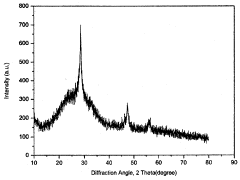
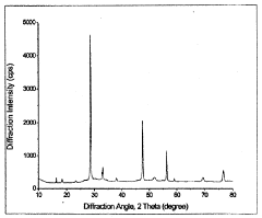
Despite significant advancements in skutterudite-based thermoelectric materials, the fabrication of high-quality skutterudite thin films remains challenging. One of the primary obstacles is achieving precise stoichiometric control during deposition processes. Skutterudites, with their complex crystal structure (CoSb3, CoP3, etc.) and multiple elements, require extremely accurate compositional control to maintain their thermoelectric properties. Even minor deviations in elemental ratios can significantly degrade performance or prevent the formation of the desired phase altogether.
Thermal stability presents another major challenge. The high vapor pressure of antimony in CoSb3-based skutterudites leads to substantial Sb loss during high-temperature deposition processes. This volatility makes it difficult to maintain the correct stoichiometry throughout the deposition process and during subsequent annealing treatments, often resulting in secondary phase formation or compositional gradients across the film thickness.
Substrate compatibility issues further complicate skutterudite thin film fabrication. The thermal expansion coefficient mismatch between skutterudite materials and common substrates can induce significant stress in the films, leading to cracking, delamination, or poor crystallinity. Additionally, chemical reactions at the film-substrate interface may occur at elevated temperatures, potentially forming unwanted compounds that degrade thermoelectric performance.
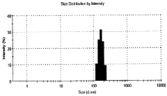
The optimization of film microstructure represents another significant challenge. Thermoelectric performance is highly dependent on grain size, orientation, and boundary characteristics. Current deposition techniques struggle to simultaneously achieve high crystallinity while maintaining nanoscale features that enhance phonon scattering without severely compromising electrical conductivity.
Doping and filling control in thin film form is particularly problematic. While bulk skutterudites benefit from the "phonon-glass electron-crystal" concept through void filling with guest atoms (like rare earth elements), precisely controlling this process in thin films remains difficult. The incorporation of dopants and fillers often occurs non-uniformly, and their tendency to segregate or diffuse during processing further complicates matters.
Scalability and reproducibility issues persist across different deposition techniques. Methods that produce high-quality films in laboratory settings often face significant challenges when scaled to larger areas or industrial production volumes. Variations in film thickness, composition, and microstructure across larger substrates remain problematic for commercial applications.
Finally, the integration of skutterudite thin films into practical devices presents additional challenges related to contact resistance, thermal stability during operation, and long-term reliability. The development of compatible electrode materials and effective barrier layers to prevent interdiffusion during device operation remains an active area of research with significant technical hurdles.
Thermal stability presents another major challenge. The high vapor pressure of antimony in CoSb3-based skutterudites leads to substantial Sb loss during high-temperature deposition processes. This volatility makes it difficult to maintain the correct stoichiometry throughout the deposition process and during subsequent annealing treatments, often resulting in secondary phase formation or compositional gradients across the film thickness.
Substrate compatibility issues further complicate skutterudite thin film fabrication. The thermal expansion coefficient mismatch between skutterudite materials and common substrates can induce significant stress in the films, leading to cracking, delamination, or poor crystallinity. Additionally, chemical reactions at the film-substrate interface may occur at elevated temperatures, potentially forming unwanted compounds that degrade thermoelectric performance.
The optimization of film microstructure represents another significant challenge. Thermoelectric performance is highly dependent on grain size, orientation, and boundary characteristics. Current deposition techniques struggle to simultaneously achieve high crystallinity while maintaining nanoscale features that enhance phonon scattering without severely compromising electrical conductivity.
Doping and filling control in thin film form is particularly problematic. While bulk skutterudites benefit from the "phonon-glass electron-crystal" concept through void filling with guest atoms (like rare earth elements), precisely controlling this process in thin films remains difficult. The incorporation of dopants and fillers often occurs non-uniformly, and their tendency to segregate or diffuse during processing further complicates matters.
Scalability and reproducibility issues persist across different deposition techniques. Methods that produce high-quality films in laboratory settings often face significant challenges when scaled to larger areas or industrial production volumes. Variations in film thickness, composition, and microstructure across larger substrates remain problematic for commercial applications.
Finally, the integration of skutterudite thin films into practical devices presents additional challenges related to contact resistance, thermal stability during operation, and long-term reliability. The development of compatible electrode materials and effective barrier layers to prevent interdiffusion during device operation remains an active area of research with significant technical hurdles.
State-of-the-Art Deposition Techniques for Skutterudites
01 Composition and structure of skutterudite thin films
Skutterudite thin films can be composed of various elements including cobalt, iron, nickel combined with antimony, arsenic, or phosphorus. The crystal structure and composition significantly affect the thermoelectric properties. These films can be engineered with specific stoichiometric ratios to optimize their thermoelectric performance. The microstructure and grain boundaries of the thin films play crucial roles in determining thermal conductivity and electrical resistivity.- Composition and structure of skutterudite thin films: Skutterudite thin films can be fabricated with various compositions and structures to enhance their thermoelectric properties. These films typically consist of CoSb3-based materials with specific dopants to optimize their performance. The structure of these films, including their crystallinity, grain size, and orientation, significantly affects their thermoelectric efficiency. Advanced deposition techniques are used to control these parameters and create high-quality skutterudite thin films with improved thermoelectric properties.
- Doping strategies for skutterudite thin films: Doping is a critical strategy for enhancing the thermoelectric properties of skutterudite thin films. Various elements, such as rare earth metals, alkaline earth metals, and transition metals, can be incorporated into the skutterudite structure to modify its electronic and thermal transport properties. These dopants can fill the voids in the skutterudite structure, reducing thermal conductivity while maintaining or improving electrical conductivity. Optimized doping concentrations and combinations can significantly increase the figure of merit (ZT) of skutterudite thin films.
- Fabrication methods for skutterudite thin films: Various fabrication methods are employed to produce skutterudite thin films with enhanced thermoelectric properties. These include physical vapor deposition techniques such as sputtering, pulsed laser deposition, and thermal evaporation, as well as chemical methods like chemical vapor deposition and electrodeposition. Post-deposition treatments, such as annealing and thermal processing, are often applied to improve crystallinity and optimize the thermoelectric performance of the films. The choice of fabrication method significantly impacts the microstructure and thermoelectric properties of skutterudite thin films.
- Nanostructuring approaches for skutterudite thin films: Nanostructuring is an effective approach to enhance the thermoelectric properties of skutterudite thin films. By introducing nanoscale features such as quantum dots, nanowires, or nanolayers, phonon scattering can be increased without significantly affecting electron transport. This leads to reduced thermal conductivity while maintaining electrical conductivity, resulting in improved thermoelectric performance. Various techniques, including multilayer deposition, nanocomposite formation, and controlled grain growth, are used to create nanostructured skutterudite thin films with enhanced thermoelectric properties.
- Device integration and performance optimization: Integrating skutterudite thin films into practical thermoelectric devices requires careful optimization of film thickness, substrate selection, and contact materials. The interfaces between the skutterudite film and other device components significantly affect overall performance. Various strategies, such as buffer layer insertion, interface engineering, and electrode optimization, are employed to maximize device efficiency. Additionally, the stability and reliability of skutterudite thin film devices under operating conditions are critical considerations for practical applications in waste heat recovery, cooling systems, and power generation.
02 Deposition techniques for skutterudite thin films
Various deposition methods are employed to fabricate skutterudite thin films with enhanced thermoelectric properties. These include physical vapor deposition (PVD), chemical vapor deposition (CVD), magnetron sputtering, pulsed laser deposition, and molecular beam epitaxy. The deposition parameters such as temperature, pressure, and deposition rate significantly influence the film quality, crystallinity, and thermoelectric performance. Post-deposition treatments like annealing can further improve the thermoelectric properties by optimizing the microstructure.Expand Specific Solutions03 Doping and filling strategies for skutterudite thin films
Doping and filling the skutterudite structure with guest atoms can significantly enhance thermoelectric properties. Common dopants include rare earth elements, alkaline earth metals, and transition metals. These dopants can reduce thermal conductivity through phonon scattering while maintaining or improving electrical conductivity. Multiple filling with different elements can create complex skutterudites with optimized thermoelectric figure of merit (ZT). Nano-inclusions and precipitates formed during doping can further enhance phonon scattering.Expand Specific Solutions04 Nanostructuring approaches for skutterudite thin films
Nanostructuring approaches are employed to enhance the thermoelectric properties of skutterudite thin films. These include creating nanolayers, quantum dots, nanoinclusions, and superlattice structures. Nanostructuring reduces thermal conductivity through increased phonon scattering at interfaces while preserving electrical conductivity. Controlled grain size and boundary engineering can optimize the power factor. Advanced techniques like selective area growth and template-assisted deposition enable precise control over nanostructure formation.Expand Specific Solutions05 Device integration and performance optimization
Integration of skutterudite thin films into thermoelectric devices requires optimization of interfaces, contacts, and overall device architecture. Techniques to reduce contact resistance between the skutterudite film and electrodes are crucial for device efficiency. Thermal stability and mechanical properties must be considered for practical applications. Multilayer structures combining different thermoelectric materials can enhance overall device performance. Testing methodologies for accurately measuring the thermoelectric properties of thin films have been developed to facilitate optimization.Expand Specific Solutions
Leading Research Groups and Industrial Players
The skutterudite thin film thermoelectric technology market is currently in an early growth phase, characterized by intensive research and development activities rather than widespread commercial deployment. The global thermoelectric materials market, valued at approximately $55 million, is expected to grow significantly as energy harvesting applications expand. Technologically, skutterudite thin film deposition remains at medium maturity, with key players advancing different approaches. Academic institutions like University of Science & Technology Beijing and Boston University are pioneering fundamental research, while companies including GlobalFoundries, Seiko Epson, and MAHLE International are developing manufacturing capabilities. Research organizations such as Shanghai Institute of Ceramics and National Center for Nanoscience & Technology are bridging the gap between theoretical advances and practical applications, focusing on improving deposition techniques and thermoelectric performance characterization.
University of Electronic Science & Technology of China
Technical Solution: University of Electronic Science & Technology of China has developed specialized RF magnetron sputtering techniques for skutterudite thin film deposition with precise control over film microstructure. Their approach incorporates reactive sputtering with controlled partial pressures to optimize film composition and reduce defects. The university has pioneered the use of gradient composition skutterudite films, where the Sb/Co ratio varies throughout the film thickness to create optimized carrier concentration profiles. Their research demonstrates successful fabrication of n-type and p-type skutterudite films on flexible substrates, opening applications in wearable thermoelectric generators. The team has developed specialized in-situ annealing chambers that allow for precise control of film crystallization without antimony loss, a common challenge in skutterudite processing. Their characterization methodology includes custom-built measurement systems for simultaneous determination of Seebeck coefficient, electrical conductivity, and thermal conductivity in thin film samples.
Strengths: Advanced control over film composition gradients; successful demonstration of films on flexible substrates; comprehensive in-house characterization capabilities for thermoelectric properties. Weaknesses: Challenges in achieving uniform properties over large areas; complex process control requirements; limited industrial partnerships for commercialization.
Tianjin University
Technical Solution: Tianjin University has developed a hybrid deposition approach for skutterudite thin films combining electrodeposition and thermal evaporation techniques. Their innovative process begins with electrodeposition of cobalt layers followed by thermal evaporation of antimony, with subsequent thermal treatment to form the skutterudite phase. This approach allows for cost-effective fabrication of relatively thick films (1-5μm) with good adhesion to metallic substrates. The university has also pioneered the use of surfactant-assisted electrodeposition to control grain size and orientation in skutterudite films, which significantly impacts thermoelectric performance. Their research demonstrates successful incorporation of multiple dopants (Fe, Ni, Te) during the deposition process to optimize carrier concentration. Tianjin University has developed specialized thermal treatment protocols that prevent antimony sublimation while promoting optimal crystallization of the skutterudite phase. Their characterization approach includes custom-built measurement systems for thin film thermoelectric properties under various temperature gradients and mechanical stresses.
Strengths: Cost-effective fabrication approach compared to vacuum-based techniques; ability to produce relatively thick films with good mechanical properties; excellent control over dopant incorporation. Weaknesses: Challenges in achieving uniform composition throughout film thickness; limited substrate compatibility compared to vacuum techniques; potential for oxidation during processing.
Critical Analysis of Thermoelectric Characterization Methods
Improved production of an energy-reflecting composite
PatentWO2023170214A1
Innovation
- A method involving sputter deposition with controlled introduction of water vapor in the sputtering chamber, adjusting the molar flow of water relative to inert gas, to optimize the transmittance spectrum by enhancing the anchoring of metal layers and altering the optical properties of dielectric layers, thereby shifting the transmittance curve towards lower wavelength ranges.

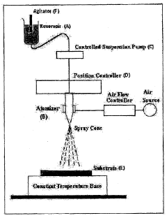
Method to deposit continuous uniform adhesive films using pre-synthesized powder material
PatentInactiveIN874KOL2014A
Innovation
- A method involving the suspension of pre-synthesized spherical seed crystals in a precursor solution, which is sprayed onto a heated substrate, utilizing ultrasonication and controlled flow to form a uniform, adhesive, and defect-free film with improved crystal growth.
Material Sustainability and Environmental Impact
The sustainability aspects of skutterudite thin films represent a critical dimension in evaluating their viability for widespread thermoelectric applications. These materials, while promising for energy harvesting and cooling technologies, contain elements such as cobalt, antimony, and rare earth metals that raise significant environmental concerns throughout their lifecycle.
Mining and extraction processes for skutterudite constituents often involve substantial energy consumption and potential environmental degradation. Particularly concerning is the extraction of antimony, which frequently results in soil contamination and water pollution if not properly managed. The carbon footprint associated with these extraction processes contributes significantly to the overall environmental impact of skutterudite-based technologies.
Deposition techniques for skutterudite thin films present varying degrees of environmental burden. Physical vapor deposition methods typically consume considerable energy, while chemical approaches may utilize toxic precursors that require careful handling and disposal. Recent research has focused on developing more environmentally benign deposition routes, including aqueous solution-based methods that operate at lower temperatures and reduce hazardous waste generation.
The recyclability of skutterudite thin films presents both challenges and opportunities. While the valuable metal content makes recovery economically attractive, the composite nature of these films and their integration into complex device architectures complicates end-of-life processing. Emerging research on selective etching techniques shows promise for separating and recovering the constituent elements with minimal environmental impact.
Life cycle assessment (LCA) studies of skutterudite-based thermoelectric devices indicate that their environmental benefits may outweigh impacts if deployed in appropriate applications. The energy harvested or saved through their operation can potentially offset the environmental costs of production, particularly in long-lifetime applications such as industrial waste heat recovery systems.
Material substitution strategies represent another important sustainability direction. Research into reducing or eliminating toxic elements like antimony while maintaining thermoelectric performance has yielded promising alternatives. Similarly, efforts to decrease reliance on scarce elements through partial substitution with earth-abundant materials may enhance long-term sustainability without significantly compromising performance.
Regulatory frameworks governing the use of potentially harmful elements in skutterudite compositions vary globally, creating challenges for international commercialization. Compliance with regulations such as RoHS in Europe and similar initiatives worldwide necessitates careful material selection and processing approaches that minimize environmental and health risks throughout the product lifecycle.
Scale-up Potential and Manufacturing Feasibility
The scale-up potential for skutterudite thin film technology represents a critical consideration for transitioning from laboratory-scale research to commercial applications. Current deposition techniques, including magnetron sputtering, pulsed laser deposition, and flash evaporation, demonstrate varying degrees of scalability. Magnetron sputtering shows particular promise for industrial implementation due to its established presence in semiconductor manufacturing and compatibility with large-area substrates.
Manufacturing feasibility analysis indicates several key challenges that must be addressed. Material uniformity across larger substrates remains problematic, with edge effects and compositional gradients becoming more pronounced as deposition area increases. The multi-element nature of skutterudite compounds (CoSb3, filled variants with rare earth elements) introduces complexity in maintaining stoichiometric precision during scaled production processes.
Equipment considerations reveal that existing industrial PVD systems could be adapted for skutterudite thin film production with moderate modifications. However, specialized monitoring systems would be required to ensure real-time composition control during deposition. Cost modeling suggests that while initial capital investment would be substantial, the per-unit manufacturing costs could decrease significantly with scale, potentially reaching economically viable levels for certain applications.
Process optimization represents another critical factor in manufacturing feasibility. Current deposition rates for high-quality skutterudite films (typically 1-5 nm/min) would need substantial improvement for commercial viability. Post-deposition annealing processes, essential for optimizing thermoelectric properties, present additional scaling challenges regarding temperature uniformity across larger substrates.
Integration with existing manufacturing workflows must also be considered. The compatibility of skutterudite thin film processes with standard microfabrication techniques would facilitate adoption in thermoelectric device manufacturing. Preliminary assessments indicate that skutterudite films could be incorporated into established semiconductor processing lines with appropriate process modifications.
Environmental and safety considerations for scaled manufacturing appear manageable but require attention. The antimony content in skutterudite compounds necessitates appropriate handling protocols, though established procedures from the semiconductor industry provide applicable frameworks. Energy consumption during deposition and annealing processes represents a significant factor in production costs that warrants optimization.
Market readiness assessment suggests that while technical feasibility exists for scaling skutterudite thin film production, economic viability currently limits immediate large-scale implementation. Targeted applications in specialized thermal management solutions and small-scale energy harvesting represent the most promising initial commercialization pathways before broader market penetration becomes feasible.
Unlock deeper insights with Patsnap Eureka Quick Research — get a full tech report to explore trends and direct your research. Try now!
Generate Your Research Report Instantly with AI Agent
Supercharge your innovation with Patsnap Eureka AI Agent Platform!