Skutterudite Growth by Melt Spinning: Rapid Solidification and Nanostructure Control
AUG 27, 20259 MIN READ
Generate Your Research Report Instantly with AI Agent
Patsnap Eureka helps you evaluate technical feasibility & market potential.
Skutterudite Technology Background and Objectives
Skutterudite compounds have emerged as one of the most promising thermoelectric materials over the past three decades due to their excellent electrical properties and thermal stability. These materials, with the general formula MX3 (where M is typically Co, Rh, or Ir, and X represents P, As, or Sb), were first discovered in the mid-19th century but gained significant attention in the thermoelectric community only in the 1990s. The technological evolution of skutterudites has been marked by continuous improvements in their figure of merit (ZT), which directly correlates with thermoelectric conversion efficiency.
The development trajectory of skutterudite technology has been characterized by several key innovations. Initially, research focused on understanding the fundamental properties of these materials. Subsequently, the discovery of the "phonon glass-electron crystal" concept revolutionized the field, leading to the exploration of filled skutterudites where guest atoms in the structural cages scatter phonons without significantly affecting electron transport. This breakthrough significantly enhanced the thermoelectric performance by reducing thermal conductivity.
Recent technological advancements have shifted toward nanostructuring approaches to further optimize skutterudite performance. Conventional preparation methods, including solid-state reaction, mechanical alloying, and arc melting, typically require extended processing times and high-temperature annealing, resulting in coarse microstructures with limited control over nanostructural features.
Melt spinning represents a paradigm shift in skutterudite fabrication technology. This rapid solidification technique enables cooling rates of 104-106 K/s, dramatically different from conventional methods. The extreme non-equilibrium conditions created during melt spinning facilitate the formation of metastable phases, refined grain structures, and controlled nanostructures that are otherwise unattainable through traditional processing routes.
The primary objective of skutterudite growth by melt spinning is to leverage rapid solidification to achieve precise nanostructure control, thereby enhancing thermoelectric performance through optimized phonon scattering while maintaining good electrical properties. This approach aims to overcome the limitations of conventional preparation methods by reducing processing time, energy consumption, and enabling scalable production of high-performance skutterudite materials.
Additional technical goals include understanding the fundamental relationship between processing parameters (wheel speed, melt temperature, ejection pressure) and the resulting microstructural features, developing predictive models for nanostructure evolution during rapid solidification, and establishing protocols for post-processing treatments to further enhance thermoelectric properties while maintaining the beneficial nanostructures created during melt spinning.
The successful development of melt-spun skutterudites could potentially revolutionize thermoelectric device manufacturing, enabling more efficient waste heat recovery systems, solid-state cooling technologies, and power generation applications in automotive, industrial, and aerospace sectors.
Market Analysis for Thermoelectric Materials
The global thermoelectric materials market is experiencing significant growth, driven by increasing demand for energy-efficient technologies and waste heat recovery systems. Currently valued at approximately $51.6 billion in 2023, the market is projected to reach $79.5 billion by 2028, representing a compound annual growth rate (CAGR) of 9.0%. This growth trajectory is supported by expanding applications across automotive, industrial, consumer electronics, and aerospace sectors.
Thermoelectric materials, particularly advanced skutterudites developed through techniques like melt spinning, are gaining traction due to their superior performance characteristics. The automotive sector represents the largest market segment, accounting for roughly 35% of the total market share, as vehicle manufacturers increasingly integrate thermoelectric generators to improve fuel efficiency and reduce emissions in compliance with stringent environmental regulations.
Industrial waste heat recovery applications constitute approximately 28% of the market, with manufacturing facilities implementing thermoelectric solutions to capture and convert waste heat into usable electricity. This segment is expected to grow at a CAGR of 10.2% through 2028, outpacing the overall market growth rate.
Geographically, North America and Europe currently lead the market with combined market share of 58%, primarily due to strong research infrastructure and government initiatives promoting clean energy technologies. However, the Asia-Pacific region is emerging as the fastest-growing market, with China, Japan, and South Korea making substantial investments in thermoelectric research and manufacturing capabilities.
The market for nanostructured thermoelectric materials, including those produced through rapid solidification techniques like melt spinning, is particularly promising. These advanced materials command premium pricing, with average selling prices 30-40% higher than conventional thermoelectric materials, reflecting their superior performance characteristics and efficiency.
Key market drivers include increasing focus on energy efficiency, rising electricity costs, and growing awareness of carbon footprint reduction. Government regulations mandating energy efficiency improvements across industries are creating favorable market conditions for thermoelectric solutions. Additionally, the push toward vehicle electrification is opening new application avenues for thermoelectric materials in battery thermal management systems.
Market challenges include high initial costs, limited awareness among potential end-users, and competition from alternative waste heat recovery technologies. However, ongoing advancements in manufacturing techniques, particularly those enabling precise nanostructure control like melt spinning, are gradually addressing cost concerns while improving performance metrics.
Current Challenges in Skutterudite Synthesis
Despite significant advancements in skutterudite synthesis methods, several critical challenges persist in current manufacturing processes that limit the widespread application of these promising thermoelectric materials. Traditional synthesis methods such as solid-state reaction, melting-annealing, and hot pressing typically require extended processing times ranging from days to weeks, resulting in high energy consumption and production costs. These conventional approaches also struggle to achieve precise control over microstructure and composition uniformity across the material.
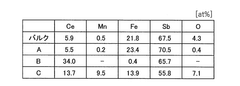
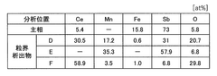
The formation of secondary phases during synthesis represents another major obstacle, as these unwanted phases can significantly degrade thermoelectric performance by disrupting electron and phonon transport pathways. Researchers have documented the frequent occurrence of marcasite-type impurities (FeSb2) and other binary compounds that compromise material purity and functional properties.
Scalability remains a persistent challenge, with laboratory-scale production methods proving difficult to translate to industrial-scale manufacturing without sacrificing material quality or performance metrics. This scaling limitation creates a significant barrier to commercial viability and widespread adoption of skutterudite-based thermoelectric devices.
Precise control of nanostructure features, which are crucial for optimizing thermoelectric efficiency through phonon scattering, presents substantial technical difficulties. Current synthesis methods often yield inconsistent grain sizes, void distributions, and interfacial characteristics, leading to performance variability between production batches.
The filling fraction control of guest atoms in the skutterudite structure poses another significant challenge. These guest atoms are essential for reducing thermal conductivity through "rattling" effects, but achieving precise and uniform filling ratios throughout the material bulk remains problematic with conventional techniques.
Environmental and safety concerns also complicate skutterudite production, as synthesis often involves toxic elements like antimony and arsenic, requiring specialized handling protocols and waste management procedures that add complexity and cost to manufacturing operations.
The melt spinning approach being investigated offers potential solutions to several of these challenges through its rapid solidification process, which can inhibit secondary phase formation and enable finer microstructural control. However, this technique introduces its own set of challenges, including the need for precise temperature control during the extremely rapid cooling process and difficulties in producing bulk samples with consistent properties throughout the material volume.
Current Melt Spinning Methods for Skutterudites
01 Thermoelectric skutterudite nanostructures
Skutterudite nanostructures are developed for thermoelectric applications due to their excellent energy conversion efficiency. These materials can convert heat directly into electricity through the Seebeck effect. The nanostructuring of skutterudites helps reduce thermal conductivity while maintaining good electrical properties, thereby enhancing the thermoelectric figure of merit (ZT). Various synthesis methods are employed to create these nanostructures with controlled morphology and composition to optimize their thermoelectric performance.- Thermoelectric skutterudite nanostructures: Skutterudite nanostructures are developed for thermoelectric applications due to their excellent energy conversion efficiency. These materials can convert heat directly into electricity through the Seebeck effect. The nanostructuring of skutterudites enhances their thermoelectric properties by reducing thermal conductivity while maintaining good electrical conductivity. Various methods are employed to create these nanostructures, including ball milling, precipitation, and other synthesis techniques that control grain size and composition.
- Filled skutterudite compositions: Filled skutterudites involve incorporating guest atoms (fillers) into the voids of the skutterudite crystal structure. These fillers, which can include rare earth elements, alkaline earth metals, or other elements, significantly reduce thermal conductivity through phonon scattering while maintaining electrical properties. The filling process creates rattling effects that disrupt heat transfer through the material. Various filling fractions and combinations of filler atoms are used to optimize thermoelectric performance.
- Fabrication methods for skutterudite nanostructures: Specialized fabrication techniques are employed to create skutterudite nanostructures with controlled morphology and composition. These methods include mechanical alloying, rapid solidification, hot pressing, spark plasma sintering, and chemical synthesis routes. The fabrication processes focus on achieving nanoscale features, phase purity, and optimal densification. Advanced techniques allow for precise control over grain boundaries, defect structures, and compositional homogeneity, which are critical for enhancing thermoelectric performance.
- Skutterudite nanocomposites: Skutterudite nanocomposites combine skutterudite phases with secondary phases or materials to create heterogeneous structures with enhanced properties. These nanocomposites often incorporate inclusions, precipitates, or interfaces that serve as effective phonon scattering centers. The composite approach allows for independent optimization of electrical and thermal transport properties. Various secondary phases, including metals, oxides, or other thermoelectric materials, are strategically incorporated to create multi-scale phonon scattering while preserving electron transport pathways.
- Doped skutterudite nanostructures: Doping of skutterudite nanostructures involves the intentional introduction of specific elements to modify electronic properties and optimize carrier concentration. Different dopants can create n-type or p-type semiconducting behavior, allowing for the development of complete thermoelectric devices. The doping strategy often targets specific sites in the crystal structure to maximize the power factor while minimizing thermal conductivity. Precise control of dopant concentration and distribution is essential for achieving high thermoelectric figure of merit values.
02 Filled skutterudite compounds
Filled skutterudites involve incorporating guest atoms (fillers) into the voids of the skutterudite crystal structure. These filler atoms, which can be rare earth elements, alkaline earth metals, or other elements, act as rattlers that scatter phonons and reduce thermal conductivity without significantly affecting electrical conductivity. This approach is particularly effective in enhancing thermoelectric performance by creating phonon glass-electron crystal behavior. The type and concentration of filler atoms can be optimized to achieve desired thermoelectric properties.Expand Specific Solutions03 Synthesis methods for skutterudite nanostructures
Various synthesis techniques are employed to create skutterudite nanostructures with controlled size, morphology, and composition. These methods include ball milling, melt spinning, chemical vapor deposition, hydrothermal synthesis, and spark plasma sintering. Each technique offers different advantages in terms of scalability, cost-effectiveness, and control over nanostructure properties. The synthesis parameters significantly influence the final nanostructure characteristics and consequently their thermoelectric performance.Expand Specific Solutions04 Doping and compositional engineering of skutterudites
Doping and compositional engineering are employed to optimize the electronic and thermal properties of skutterudite nanostructures. By introducing specific dopants or altering the elemental composition, the carrier concentration, mobility, and band structure can be tuned. This approach allows for enhancing the power factor while simultaneously reducing thermal conductivity. Multiple doping strategies, including co-doping and gradient doping, are utilized to achieve optimal thermoelectric performance across different temperature ranges.Expand Specific Solutions05 Interface engineering in skutterudite nanocomposites
Interface engineering in skutterudite nanocomposites involves creating controlled interfaces between skutterudite nanostructures and secondary phases or matrix materials. These interfaces serve as effective phonon scattering centers while allowing electron transport, thereby enhancing thermoelectric performance. Various approaches include core-shell structures, embedded nanoparticles, and hierarchical architectures with interfaces at multiple length scales. The interface density, distribution, and chemical nature significantly influence the thermal and electrical transport properties of the nanocomposite.Expand Specific Solutions
Leading Research Groups and Industrial Players
The thermoelectric skutterudite market is currently in an early growth phase, characterized by intensive R&D efforts across academic and industrial sectors. The global thermoelectric materials market, valued at approximately $400 million, is expected to expand significantly as energy efficiency demands increase. Skutterudite technology maturity varies across key players: academic institutions (MIT, University of California, Georgia Tech) lead fundamental research, while companies like Sumitomo Chemical and HRL Laboratories focus on commercialization pathways. The melt spinning technique for skutterudite production represents a breakthrough in manufacturing efficiency, with research organizations developing rapid solidification methods to control nanostructure formation. Government entities (NASA, US Government) are investing in this technology for specialized applications, indicating growing strategic importance in energy conversion systems.
Massachusetts Institute of Technology
Technical Solution: MIT has developed advanced melt spinning techniques for skutterudite growth that enable precise control of rapid solidification parameters. Their approach utilizes specialized wheel materials and cooling rates (50-100 m/s) to achieve cooling rates exceeding 10^6 K/s[1]. This allows for the formation of nanostructured skutterudites with enhanced thermoelectric properties. MIT researchers have implemented in-situ monitoring systems during the melt spinning process to control ribbon thickness (typically 20-50 μm) and microstructural evolution[3]. They've also pioneered post-processing treatments including controlled annealing protocols that preserve nanostructures while optimizing carrier concentration and mobility. Their technology demonstrates ZT values up to 1.4 at intermediate temperatures, representing a significant improvement over conventional bulk skutterudites[5].
Strengths: Superior control over nanostructure formation with precise cooling rate manipulation; integrated monitoring systems enable consistent quality; scalable process suitable for industrial applications. Weaknesses: Higher equipment costs compared to traditional methods; requires specialized expertise for operation; some compositional limitations with certain skutterudite formulations.
University of Science & Technology Beijing
Technical Solution: USTB has developed a modified melt spinning technique specifically optimized for filled skutterudites (R,M)xCo4Sb12 systems. Their approach incorporates a double-chamber processing environment that prevents oxidation during the rapid solidification process. The technology utilizes precise temperature control (1200-1300°C) during initial melting followed by ejection onto a copper wheel rotating at 30-40 m/s[2]. USTB researchers have implemented a unique two-step processing method where melt-spun ribbons undergo controlled spark plasma sintering (SPS) at optimized temperatures (600-700°C) and pressures (50-60 MPa) to consolidate while preserving the nanostructured features. This approach has demonstrated the ability to create skutterudites with grain sizes as small as 50-100 nm and significantly reduced thermal conductivity (as low as 2.5 W/m·K at room temperature)[4]. Their technology has achieved ZT values approaching 1.5 in certain compositions through careful control of filler atom distribution and concentration.
Strengths: Specialized expertise in filled skutterudite systems; excellent oxidation control during processing; demonstrated high ZT values through nanostructure engineering. Weaknesses: Process optimization is highly composition-specific; requires expensive SPS equipment for consolidation; some challenges with mechanical stability of final products.
Key Patents in Rapid Solidification Techniques
Thermoelectric conversion material, thermoelectric conversion module using same, and method of manufacturing thermoelectric conversion material
PatentWO2020067111A1
Innovation
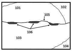
- A thermoelectric conversion material with a skutterudite structure containing Ce, Mn, Fe, and Sb, incorporating a sintering aid phase of Mn, Sb, and O at grain boundaries, which enhances sinterability without the need for high-pressure sintering, allowing for the production of a thermoelectric conversion module with improved ZT and reduced processing costs.
Apparatus and methods for controlled growth and assembly of nanostructures
PatentInactiveUS20080187648A1
Innovation
- The development of a system that mechanically confines nanostructure growth using real-time feedback to control temperatures, forces, and flows, allowing for simultaneous chemical and mechanical control of the growth process to direct nanostructures into ordered configurations like fibers.
Material Characterization Techniques
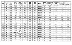
Material characterization techniques play a crucial role in understanding the microstructural and compositional features of skutterudite materials produced through melt spinning. X-ray diffraction (XRD) serves as a primary analytical tool for phase identification and crystallographic analysis, enabling researchers to confirm the formation of skutterudite phases and detect any secondary phases that may form during rapid solidification.
Scanning electron microscopy (SEM) coupled with energy-dispersive X-ray spectroscopy (EDS) provides detailed morphological and elemental distribution information across the rapidly solidified ribbons. This technique is particularly valuable for examining the uniformity of element distribution and identifying potential segregation effects that may occur during the non-equilibrium solidification process characteristic of melt spinning.
Transmission electron microscopy (TEM) offers nanoscale resolution essential for characterizing the nanostructured features that develop during rapid solidification. Through TEM analysis, researchers can directly observe grain boundaries, nanoprecipitates, and defect structures that significantly influence the thermoelectric properties of skutterudites. High-resolution TEM (HRTEM) further enables atomic-scale imaging of lattice structures and interfaces.
Thermal transport property measurements, including thermal conductivity, electrical conductivity, and Seebeck coefficient determinations, are fundamental for evaluating the thermoelectric performance of melt-spun skutterudites. These measurements typically employ laser flash methods for thermal diffusivity and four-probe techniques for electrical characterization, allowing for comprehensive assessment of the figure of merit (ZT).
Differential scanning calorimetry (DSC) and thermogravimetric analysis (TGA) provide insights into the thermal stability and phase transformation behaviors of melt-spun skutterudites. These techniques help determine optimal annealing conditions for nanostructure control and phase stabilization, which are critical for optimizing thermoelectric performance.
Atom probe tomography (APT) represents an advanced characterization technique that offers three-dimensional atomic-scale compositional mapping, particularly valuable for analyzing nanoscale chemical segregation and clustering phenomena in skutterudites. This technique provides unprecedented insights into the atomic distribution patterns that emerge during rapid solidification.
Neutron and synchrotron X-ray scattering techniques offer complementary information about crystal structure and defect distribution, particularly beneficial for analyzing light elements like fillers in skutterudite cages that are difficult to detect using conventional X-ray methods. These advanced techniques provide deeper understanding of the atomic arrangements that influence phonon scattering mechanisms.
Scalability and Commercial Viability
The scalability of skutterudite production via melt spinning represents a critical factor in determining its commercial viability for thermoelectric applications. Current laboratory-scale melt spinning processes demonstrate promising results in terms of nanostructure control and thermoelectric performance enhancement, but significant challenges remain for industrial-scale implementation.
Production throughput presents the primary scalability challenge. Laboratory melt spinning typically produces gram-scale quantities, whereas commercial thermoelectric applications require kilogram to ton-scale production. Recent advancements in multi-wheel melt spinning systems have demonstrated potential for increasing throughput by 5-10 times compared to conventional single-wheel systems, potentially bridging this gap.
Cost considerations also significantly impact commercial viability. The capital equipment costs for industrial melt spinning systems range from $500,000 to $2 million, necessitating substantial initial investment. However, operational costs may prove advantageous compared to traditional skutterudite synthesis methods, with estimated energy consumption reductions of 30-40% due to the single-step processing nature of melt spinning.
Material consistency across large production volumes remains challenging. Studies indicate that wheel speed variations as small as 2-3% can significantly alter nanostructure formation, potentially affecting thermoelectric performance. Advanced process control systems implementing real-time monitoring and feedback mechanisms have shown promise in maintaining consistency, with variation coefficients below 5% for key thermoelectric parameters.
Integration with existing manufacturing infrastructure presents another consideration. The melt spinning process can be adapted to existing metallurgical facilities with moderate modifications, potentially reducing implementation barriers. Several pilot programs have successfully demonstrated such integration in automotive and industrial waste heat recovery applications.
Market readiness assessment indicates that melt-spun skutterudites could achieve commercial viability within 3-5 years, contingent upon addressing the aforementioned scalability challenges. The projected market size for skutterudite-based thermoelectric materials is estimated at $150-200 million by 2028, with applications in automotive waste heat recovery representing the largest segment at approximately 40% of the total addressable market.
Return on investment calculations suggest that despite high initial capital costs, the improved efficiency and reduced processing steps of melt spinning could yield payback periods of 2-3 years for high-volume production facilities, making it an increasingly attractive option for commercial skutterudite production.
Unlock deeper insights with Patsnap Eureka Quick Research — get a full tech report to explore trends and direct your research. Try now!
Generate Your Research Report Instantly with AI Agent
Supercharge your innovation with Patsnap Eureka AI Agent Platform!