How to Do Thermal-Mechanical Co-Design for MV PCBs — Warpage & CTE
AUG 28, 20259 MIN READ
Generate Your Research Report Instantly with AI Agent
Patsnap Eureka helps you evaluate technical feasibility & market potential.
Thermal-Mechanical Co-Design Background and Objectives
Thermal-mechanical co-design for Medium Voltage (MV) Printed Circuit Boards (PCBs) has evolved significantly over the past three decades, driven by increasing power densities, miniaturization trends, and reliability requirements in power electronics applications. Initially, thermal and mechanical designs were treated as separate disciplines, with thermal engineers focusing on heat dissipation while mechanical engineers addressed structural integrity independently.
The evolution toward integrated co-design began in the early 2000s when the electronics industry recognized that thermal gradients significantly impact mechanical behavior, particularly in high-power applications. This realization coincided with the development of more sophisticated simulation tools capable of coupling thermal and mechanical analyses, enabling engineers to predict warpage and stress distributions under various operating conditions.
Medium voltage PCBs present unique challenges due to their operation in environments with substantial temperature fluctuations, high current densities, and strict reliability requirements. The coefficient of thermal expansion (CTE) mismatch between different materials in the PCB stack-up has emerged as a critical concern, leading to warpage, delamination, and solder joint failures that compromise both performance and longevity.
Recent technological advancements have focused on developing materials with controlled CTE values and enhanced thermal conductivity. Simultaneously, design methodologies have evolved to incorporate thermal-mechanical considerations from the earliest stages of the development process rather than as an afterthought. This paradigm shift represents a fundamental change in how MV PCBs are conceptualized and engineered.
The primary objective of thermal-mechanical co-design is to create MV PCBs that maintain dimensional stability and structural integrity across their entire operational temperature range while efficiently managing heat dissipation. This requires balancing multiple competing factors including electrical performance, thermal management, mechanical reliability, and manufacturing constraints.
Secondary objectives include minimizing warpage during assembly processes such as reflow soldering, reducing residual stresses in the finished product, and extending the operational lifetime through improved thermal cycling resistance. These objectives align with industry trends toward higher reliability standards and reduced maintenance requirements for medium voltage equipment.
The technical goals for advanced co-design methodologies include developing predictive models that accurately capture the complex interactions between thermal gradients and mechanical stresses, creating design rules that can be implemented early in the development cycle, and establishing validation protocols that verify both thermal and mechanical performance under realistic operating conditions.
As power electronics continue to advance toward higher voltages, frequencies, and power densities, the importance of thermal-mechanical co-design will only increase, making it a critical competency for companies developing next-generation MV PCB technologies.
Market Demands for MV PCB Warpage Control
The market for Medium Voltage (MV) PCBs is experiencing significant growth driven by the rapid expansion of power electronics applications in renewable energy, electric vehicles, industrial automation, and smart grid systems. These applications demand PCBs that can reliably handle higher voltages while maintaining dimensional stability under thermal stress. Industry reports indicate that the global MV PCB market is projected to grow at a compound annual growth rate of 7.2% through 2028, with particular acceleration in automotive and renewable energy sectors.
Warpage control has emerged as a critical requirement as MV PCB applications become more sophisticated. The miniaturization trend in power electronics has led to higher component densities and thinner board profiles, making warpage issues more pronounced and problematic. Manufacturing surveys reveal that warpage-related defects account for approximately 18% of all PCB assembly failures in MV applications, representing a significant yield and reliability concern.
The automotive industry, particularly electric vehicle manufacturers, has established stringent specifications for PCB flatness, typically requiring warpage values below 0.7% of the diagonal length. This demand is driven by the need for reliable high-power connections in battery management systems and power conversion modules where thermal cycling is frequent and intense.
Renewable energy systems present another major market segment with critical warpage control requirements. Solar inverters and wind power converters operate under variable load conditions that create thermal cycling stresses. Field data shows that PCB warpage-induced connection failures account for nearly 14% of maintenance events in these systems, driving demand for thermally stable board designs.
Industrial automation applications require MV PCBs with exceptional dimensional stability for motor drives and power distribution systems. The market increasingly demands boards that can maintain flatness across operating temperatures ranging from -40°C to +125°C, with minimal CTE mismatch between components and substrate materials.
The telecommunications infrastructure market, particularly with the rollout of 5G technology, has created demand for MV PCBs with improved thermal management and warpage resistance. Base station power amplifiers and distribution systems require boards that can handle both high power density and maintain signal integrity through consistent impedance characteristics that would otherwise be compromised by warpage.
Market research indicates that customers are willing to pay a premium of 15-20% for MV PCBs with guaranteed warpage specifications and thermal cycling resistance. This premium reflects the downstream cost savings from improved assembly yields, reduced field failures, and extended product lifetimes that result from effective warpage control.
Current Challenges in PCB Thermal-Mechanical Design
The thermal-mechanical co-design of medium voltage (MV) PCBs faces significant challenges due to the complex interplay between thermal management and mechanical stability. As power densities increase and form factors shrink, engineers must contend with warpage issues that can compromise electrical connections and overall reliability. The coefficient of thermal expansion (CTE) mismatch between different materials used in PCB construction creates internal stresses during thermal cycling, leading to deformation and potential failure.
One of the primary challenges is the accurate prediction of warpage behavior across varying operational conditions. Current simulation tools often struggle to model the non-linear material properties and complex geometries of modern PCB designs. The industry lacks standardized methodologies for integrating thermal and mechanical analyses into a unified workflow, resulting in siloed approaches that fail to capture critical interdependencies.
Material selection presents another significant hurdle. Traditional FR-4 substrates exhibit relatively high CTE values (14-17 ppm/°C), creating substantial mismatch with copper traces (17 ppm/°C) and component materials like silicon (2.6 ppm/°C). While advanced materials such as polyimide and ceramic-filled composites offer improved thermal stability, they introduce manufacturing complexities and cost implications that must be carefully balanced against performance requirements.
Manufacturing processes further complicate thermal-mechanical design. Reflow soldering subjects the PCB to extreme temperature gradients, inducing residual stresses that can manifest as warpage during subsequent thermal cycling. The increasing adoption of lead-free solders with higher melting points exacerbates these challenges, requiring more robust design approaches to maintain dimensional stability.
For MV applications specifically, the challenges are amplified by higher voltage isolation requirements and increased power dissipation. Designers must maintain adequate creepage and clearance distances while managing thermal hotspots that can accelerate material degradation and CTE-related failures. The integration of power components with sensitive control circuitry creates competing design constraints that are difficult to reconcile.
Testing and validation methodologies also present significant challenges. Current industry standards for warpage measurement, such as shadow moiré and digital image correlation, provide valuable data but are typically applied too late in the development cycle to inform fundamental design decisions. Real-time monitoring of thermal-mechanical behavior remains elusive, limiting engineers' ability to validate simulation models against actual performance.
Finally, the increasing complexity of PCB designs, with higher layer counts and embedded components, creates new thermal-mechanical interactions that are poorly understood. As the industry moves toward more integrated solutions, the need for comprehensive co-design approaches becomes increasingly critical to ensure reliability and performance in demanding MV applications.
Existing Thermal-Mechanical Co-Design Methodologies
01 Material selection for CTE matching in PCB design
Selecting materials with compatible coefficients of thermal expansion (CTE) is crucial for minimizing warpage in medium voltage (MV) PCBs. By carefully matching the CTE values of different materials used in the PCB stack-up, designers can reduce thermal stress during temperature cycling. This approach involves using specialized substrate materials, reinforcement fibers, and resin systems that work together to maintain dimensional stability across operating temperature ranges.- Material selection for CTE matching in PCB design: Selecting materials with compatible coefficients of thermal expansion (CTE) is crucial for minimizing warpage in medium voltage (MV) PCBs. By carefully matching the CTE values of different materials used in the PCB stack-up, designers can reduce thermal stress during temperature cycling. This approach involves selecting appropriate substrate materials, reinforcement fibers, and resin systems that work together to maintain dimensional stability across operating temperature ranges.
- Thermal simulation and modeling techniques for PCB warpage prediction: Advanced thermal simulation and modeling techniques enable designers to predict and mitigate PCB warpage before manufacturing. These computational methods analyze the thermal-mechanical behavior of PCB assemblies under various operating conditions, allowing for optimization of design parameters. Finite element analysis (FEA) and computational fluid dynamics (CFD) simulations help identify potential warpage issues and evaluate different design solutions to ensure reliable performance of MV PCBs.
- Layered structure optimization for warpage control: Optimizing the layered structure of PCBs is essential for controlling warpage in medium voltage applications. This involves strategic arrangement of copper layers, prepreg materials, and core materials to create a balanced construction that minimizes internal stresses. Techniques such as symmetrical layer stacking, graduated thicknesses, and strategic placement of high-CTE components help distribute thermal stresses evenly throughout the board, reducing the tendency for warpage during thermal cycling.
- Thermal management systems for MV PCB applications: Implementing effective thermal management systems is critical for controlling temperature distribution and reducing warpage in MV PCBs. These systems include heat sinks, thermal vias, embedded cooling channels, and specialized thermal interface materials that help dissipate heat more efficiently. By maintaining more uniform temperature profiles across the board, these thermal management solutions minimize the differential expansion that leads to warpage while improving overall reliability and performance of medium voltage PCB assemblies.
- Manufacturing process optimization for warpage reduction: Optimizing manufacturing processes plays a significant role in reducing warpage in MV PCBs. This includes controlling parameters such as lamination pressure, curing temperature profiles, cooling rates, and post-processing techniques. Advanced manufacturing methods like sequential lamination, controlled prepreg staging, and specialized fixturing during assembly help minimize residual stresses in the finished board. These process optimizations work in conjunction with material selection and design considerations to produce MV PCBs with improved dimensional stability.
02 Thermal simulation and modeling techniques
Advanced thermal simulation and modeling techniques are essential for predicting and mitigating warpage in MV PCBs. These computational methods allow designers to analyze thermal distribution, identify hotspots, and simulate mechanical stresses before physical prototyping. By integrating thermal and mechanical analyses in the design phase, engineers can optimize component placement, layer stack-up, and cooling solutions to minimize warpage effects under various operating conditions.Expand Specific Solutions03 Structural reinforcement and constraint systems
Implementing structural reinforcement and mechanical constraint systems helps control PCB warpage in medium voltage applications. These designs incorporate stiffeners, frames, or embedded support structures that provide mechanical stability while accommodating thermal expansion. Strategic placement of mounting points and the use of flexible interfaces between rigid components can significantly reduce stress concentration and prevent deformation during thermal cycling.Expand Specific Solutions04 Layer stack-up optimization for thermal management
Optimizing the PCB layer stack-up configuration is critical for effective thermal management and warpage control. This approach involves strategic arrangement of copper layers, dielectric materials, and thermal vias to create balanced thermal distribution. By designing symmetrical layer structures with appropriate thickness ratios and incorporating thermal dissipation paths, engineers can minimize temperature gradients across the board and reduce thermally-induced mechanical stress.Expand Specific Solutions05 Advanced manufacturing processes for warpage reduction
Specialized manufacturing processes can significantly reduce warpage in MV PCBs with challenging CTE requirements. These techniques include controlled lamination cycles, sequential build-up methods, and stress-relief procedures during fabrication. Post-processing treatments such as annealing or controlled cooling can also help minimize residual stresses. Additionally, innovative assembly methods that account for thermal expansion characteristics ensure that the final product maintains dimensional stability throughout its operational life.Expand Specific Solutions
Leading Companies in PCB Design and Manufacturing
The thermal-mechanical co-design for MV PCBs market is in a growth phase, driven by increasing demand for reliable high-performance electronics across multiple industries. The market is expanding as warpage and CTE (Coefficient of Thermal Expansion) challenges become critical in miniaturized, multi-layer PCB designs. Leading technology companies like Texas Instruments, Intel, and AT&S are advancing solutions through materials innovation and simulation technologies. Research institutions including Southeast University and Nanjing University of Aeronautics & Astronautics are contributing fundamental research. Automotive players such as Toyota, Bosch, and MAHLE are driving adoption as vehicle electronics complexity increases. The technology is maturing rapidly with collaborative efforts between materials suppliers like BASF and electronics manufacturers, focusing on predictive modeling and advanced composite materials to mitigate thermal stress issues.
AT & S Austria Technologie & Systemtechnik AG
Technical Solution: AT&S has developed an advanced thermal-mechanical co-design approach for MV PCBs that focuses on warpage control and CTE management. Their solution incorporates a multi-layer material stack optimization technique where they strategically place high-Tg (glass transition temperature) materials in critical layers to minimize warpage during thermal cycling. AT&S employs embedded cooling technology with copper-filled microvias and thermal vias arranged in optimized patterns to efficiently dissipate heat while maintaining structural integrity. Their proprietary "balanced lamination" process ensures symmetrical construction of PCB layers around the central core, significantly reducing warpage by up to 40% compared to conventional designs. Additionally, AT&S utilizes computational fluid dynamics (CFD) coupled with finite element analysis (FEA) to predict thermal-mechanical behavior during manufacturing and operation, allowing for design optimization before physical prototyping.
Strengths: Industry-leading expertise in high-density interconnect (HDI) and substrate-like PCBs with excellent thermal management capabilities. Their balanced lamination approach effectively minimizes warpage in complex designs. Weaknesses: Their advanced solutions typically come at premium costs and may require specialized manufacturing equipment, potentially limiting accessibility for smaller volume productions.
Texas Instruments Incorporated
Technical Solution: Texas Instruments has pioneered a comprehensive thermal-mechanical co-design methodology for MV PCBs that addresses warpage and CTE mismatch challenges. Their approach integrates material selection with structural design optimization through their "TI-PCB Thermal Integrity Framework." This framework employs a hierarchical simulation model that simultaneously evaluates thermal performance and mechanical stress across multiple physical scales. TI's solution incorporates strategic use of copper balancing techniques where copper distribution is carefully calculated across all PCB layers to minimize warpage during reflow processes. They've developed specialized thermal vias with optimized geometries and plating techniques that maintain mechanical integrity while enhancing heat dissipation by up to 30%. Additionally, TI implements a "stress-relief boundary design" methodology where board outlines and component placement are specifically engineered to reduce stress concentration points, particularly important for automotive and industrial applications where temperature cycling is severe.
Strengths: Exceptional integration of thermal simulation with mechanical stress analysis, allowing for highly accurate prediction of PCB behavior under various operating conditions. Their solutions are particularly effective for high-power applications requiring excellent reliability. Weaknesses: Implementation requires sophisticated design tools and expertise, potentially increasing development time and costs for complex designs.
Critical Technologies for Warpage and CTE Management
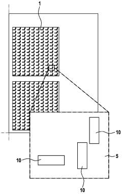
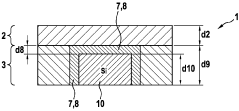
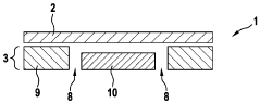
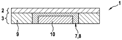
Controlling and minimizing warpage of printed circuit boards, such as asymmetric embedded component pcbs
PatentWO2024120816A1
Innovation
- A comprehensive simulation model is used to optimize the geometric and physical properties of all layers, allowing for iterative adjustments of material properties and processing parameters to minimize warpage, employing a computer-implemented method that accounts for all relevant material and geometric properties in the stack.
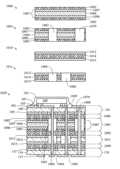
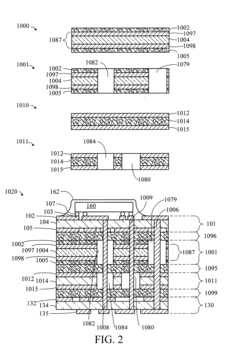
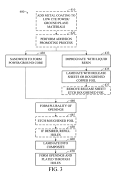
Method for making printed circuit board having low coefficient of thermal expansion power/ground plane
PatentInactiveUS6722031B2
Innovation
- The use of conductive materials with low CTEs, such as metallized carbon, graphite, glass, and liquid crystal polymer fibers, which are formed into fabrics or cores and laminated into PCBs and LCCs, providing a low CTE power and ground plane solution that reduces overall CTE and eliminates manufacturing complications associated with exotic metals.
Material Selection Strategies for Optimal CTE Matching
Material selection represents a critical foundation for effective thermal-mechanical co-design in medium voltage (MV) PCBs. The primary challenge lies in selecting materials with compatible Coefficients of Thermal Expansion (CTE) to minimize warpage during thermal cycling. Industry best practices focus on a layered approach to material selection, beginning with substrate materials that offer balanced thermal and mechanical properties.
FR-4 remains the industry standard for many applications, offering CTE values between 14-17 ppm/°C in the x-y plane. However, for MV applications requiring enhanced thermal stability, advanced materials such as polyimide (PI) with CTE values of 12-16 ppm/°C or ceramic-filled hydrocarbon laminates with CTEs as low as 8-10 ppm/°C demonstrate superior performance under thermal stress.
Copper foil selection also plays a crucial role in CTE matching strategies. Standard electrodeposited (ED) copper has a CTE of approximately 17 ppm/°C, while rolled-annealed (RA) copper offers improved ductility and fatigue resistance. For critical MV applications, specialized copper alloys with modified CTE characteristics can be employed to better match surrounding materials.
The implementation of glass-reinforced prepregs with tailored fiber orientations provides another dimension of CTE control. By strategically orienting glass fibers in multiple directions, engineers can create more isotropic thermal expansion behavior, reducing directional warpage tendencies that commonly plague MV PCBs operating in variable thermal environments.
Composite material systems represent the cutting edge of CTE matching strategies. These systems incorporate nano-fillers such as silicon carbide, aluminum nitride, or boron nitride into the resin matrix, allowing precise engineering of the resulting CTE. The concentration of these fillers can be adjusted to achieve CTE values ranging from 6-14 ppm/°C, enabling close matching with copper and other conductive elements.
For interconnect regions, where CTE mismatches are most problematic, gradient material approaches have shown promising results. These techniques involve creating transitional zones between materials with significantly different CTEs, thereby distributing thermal stress over a larger area rather than concentrating it at abrupt material boundaries.
Recent advancements in material science have introduced self-compensating material systems that actively counteract thermal expansion through opposing mechanical mechanisms. These innovative materials incorporate micro-structures that exhibit negative thermal expansion in specific directions, effectively neutralizing the positive expansion of traditional PCB materials.
Industry Standards and Reliability Testing Protocols
The thermal-mechanical co-design of Medium Voltage (MV) PCBs requires adherence to stringent industry standards and reliability testing protocols to ensure operational safety and longevity. IPC-6012, specifically Class 3 for high-reliability electronic products, serves as the foundational standard governing PCB manufacturing quality and reliability requirements for MV applications. This standard outlines specific parameters for thermal cycling resistance, dimensional stability, and material integrity that directly impact warpage and CTE management.
For thermal performance assessment, IPC-TM-650 provides test methods that evaluate PCB behavior under thermal stress. Method 2.6.8 specifically addresses thermal stress testing, while Method 2.4.24 covers glass transition temperature determination—critical for understanding material behavior across operational temperature ranges. These standardized tests help engineers quantify the thermal expansion characteristics that contribute to warpage issues.
JEDEC standards, particularly JESD22-A104 for temperature cycling and JESD22-B106 for board-level drop testing, offer complementary protocols for evaluating the reliability of PCB assemblies under thermal and mechanical stresses. These standards are essential for validating designs intended for environments with significant temperature fluctuations, where CTE mismatch becomes most problematic.
The IEC 61189 series provides additional testing methodologies specifically relevant to electrical insulation and physical endurance of PCBs. Part 2 of this standard addresses test methods for materials and assemblies, including thermal shock resistance (Test 2E) and dimensional stability assessments (Test 2M) that directly correlate with warpage prevention strategies.
Reliability qualification testing typically follows a structured approach including High Accelerated Thermal Shock (HATS), Highly Accelerated Stress Test (HAST), and Temperature Humidity Bias (THB) testing. These accelerated aging tests simulate years of operational stress in compressed timeframes, allowing engineers to identify potential failure modes related to CTE mismatch and warpage before field deployment.
For MV applications specifically, additional standards such as IEC 60664 for insulation coordination and UL 746E for industrial laminates become relevant, as they address electrical spacing and material performance under elevated voltage conditions. These standards inform material selection decisions that balance thermal-mechanical properties with electrical insulation requirements.
Compliance with these standards and testing protocols not only ensures regulatory acceptance but also provides a systematic framework for thermal-mechanical co-design optimization. By leveraging these established methodologies, engineers can develop quantifiable metrics for warpage control and CTE management that lead to more reliable MV PCB designs with predictable long-term performance characteristics.
Unlock deeper insights with Patsnap Eureka Quick Research — get a full tech report to explore trends and direct your research. Try now!
Generate Your Research Report Instantly with AI Agent
Supercharge your innovation with Patsnap Eureka AI Agent Platform!