SiC vs GaN for SST Power Stages: Voltage Classes, Switching Speed and Loss
AUG 28, 20259 MIN READ
Generate Your Research Report Instantly with AI Agent
Patsnap Eureka helps you evaluate technical feasibility & market potential.
SiC and GaN Power Technologies Background and Objectives
Silicon Carbide (SiC) and Gallium Nitride (GaN) have emerged as revolutionary wide bandgap (WBG) semiconductor materials that are transforming power electronics. The evolution of these technologies spans several decades, with significant acceleration in commercial adoption occurring in the past ten years. SiC technology development began in the 1990s, while GaN power devices gained momentum in the early 2000s. Both technologies represent a paradigm shift from traditional silicon-based power semiconductors, offering superior performance characteristics that enable more efficient power conversion systems.
The technological trajectory of these WBG materials has been driven by increasing demands for higher efficiency, power density, and reliability in power conversion applications. SiC has established a strong presence in higher voltage applications (>650V), while GaN has demonstrated exceptional performance in the 100-650V range. This differentiation in voltage classes has shaped their respective market positions and application focuses.
Recent advancements in manufacturing processes have significantly reduced production costs and improved device quality, accelerating the transition from silicon to WBG semiconductors. The compound annual growth rate (CAGR) for SiC and GaN power devices is projected to exceed 30% through 2026, indicating strong market confidence in these technologies.
The primary technical objective in comparing SiC and GaN for Solid-State Technology (SST) power stages is to determine the optimal material choice based on specific application requirements. This involves comprehensive analysis of their performance across different voltage classes, switching frequencies, and loss profiles. SiC devices typically offer robust performance at higher voltages with excellent thermal conductivity, while GaN excels in high-frequency applications with minimal switching losses.
Understanding the fundamental material properties that drive these performance differences is crucial. SiC features a bandgap of 3.2 eV and critical electric field strength of 2.8 MV/cm, compared to silicon's 1.1 eV and 0.3 MV/cm. GaN pushes these boundaries even further with a 3.4 eV bandgap and 3.3 MV/cm critical field strength. These properties directly influence the devices' voltage handling capabilities, on-resistance, and switching characteristics.
The technological goals for both SiC and GaN include further reducing specific on-resistance, improving thermal management, enhancing reliability, and lowering manufacturing costs. Additionally, developing optimized gate driver technologies and packaging solutions specifically designed for the unique characteristics of these materials represents a critical area for advancement to fully realize their potential in next-generation power conversion systems.
Market Demand Analysis for Wide Bandgap Semiconductors
The wide bandgap (WBG) semiconductor market is experiencing unprecedented growth, driven primarily by the increasing demand for high-efficiency power electronics across multiple industries. The global WBG semiconductor market was valued at approximately $1.3 billion in 2022 and is projected to reach $7.5 billion by 2030, representing a compound annual growth rate (CAGR) of 25.4% during the forecast period.
Silicon Carbide (SiC) and Gallium Nitride (GaN) technologies are at the forefront of this market expansion, particularly in solid-state power stages. The automotive sector constitutes the largest market segment, accounting for nearly 60% of the total WBG semiconductor demand. This is primarily due to the rapid adoption of electric vehicles (EVs), where SiC-based power modules offer significant advantages in high-voltage applications (650V-1700V), enabling faster charging capabilities and extended driving ranges.
Industrial applications represent the second-largest market segment at 22%, where both SiC and GaN technologies are gaining traction in motor drives, industrial power supplies, and renewable energy systems. The renewable energy sector alone is expected to grow at a CAGR of 32% through 2030, creating substantial demand for high-efficiency power conversion solutions.
Consumer electronics and telecommunications infrastructure are emerging as significant growth areas for GaN technology specifically. GaN excels in the 100V-650V range with superior switching speeds (up to 100MHz compared to SiC's typical 100kHz), making it ideal for compact, high-frequency applications such as fast chargers, data center power supplies, and 5G infrastructure.
Regional analysis indicates that Asia-Pacific dominates the WBG semiconductor market with a 45% share, followed by North America (28%) and Europe (22%). China's aggressive investment in electric vehicle manufacturing and renewable energy has positioned it as the fastest-growing market for WBG semiconductors, with a projected CAGR of 29% through 2030.
Customer demand is increasingly driven by efficiency requirements, with end-users seeking to reduce switching losses by up to 75% compared to traditional silicon solutions. This efficiency advantage translates directly to reduced cooling requirements, smaller form factors, and lower total system costs despite the higher initial component price of WBG semiconductors.
Market research indicates that the price premium for WBG solutions is steadily decreasing, with SiC components now approximately 2.5 times the cost of equivalent silicon devices, down from 5 times in 2018. GaN components show a similar trend, with price premiums expected to decrease further as manufacturing scales increase and yield improvements continue.
The market is also witnessing increased demand for integrated power modules that combine WBG semiconductors with optimized gate drivers and protection circuits, simplifying design implementation and accelerating time-to-market for end products.
Technical Challenges in SiC and GaN Power Stage Implementation
The implementation of both Silicon Carbide (SiC) and Gallium Nitride (GaN) technologies in Solid-State Transformer (SST) power stages presents significant technical challenges that must be addressed for optimal performance. Despite their superior properties compared to traditional silicon, these wide bandgap semiconductors face several critical hurdles in practical applications.
Material quality and defect density remain persistent challenges, particularly for SiC. Crystal defects such as micropipes, stacking faults, and basal plane dislocations can significantly impact device reliability and performance under high-voltage stress conditions. For GaN, the lack of native substrates necessitates heteroepitaxial growth on foreign substrates like silicon, introducing lattice mismatches that create defects and strain.
Device design optimization presents another substantial challenge. SiC MOSFETs struggle with channel mobility issues and gate oxide reliability at the SiC/SiO2 interface, requiring specialized processing techniques to minimize interface traps. GaN HEMTs face challenges with dynamic on-resistance (Ron) degradation due to charge trapping phenomena, particularly in high-voltage applications where current collapse can significantly impact switching performance.
Thermal management represents a critical challenge for both technologies. While both materials offer superior thermal conductivity compared to silicon, the higher power densities achievable with these devices create intense thermal hotspots. SiC benefits from better thermal conductivity (3-4× that of silicon), but GaN devices often require more sophisticated thermal solutions, especially when implemented on silicon substrates with thermal boundary resistance issues.
Packaging technology limitations significantly constrain the full potential of both SiC and GaN devices. Conventional packaging introduces parasitic inductances that limit switching speeds and increase losses. Advanced packaging solutions like embedded die technology and low-inductance designs are necessary but add complexity and cost to manufacturing processes.
Gate driver integration presents unique challenges for each technology. SiC devices typically require higher gate drive voltages (15-20V) with negative turn-off voltages to prevent parasitic turn-on, while GaN devices operate with lower gate voltages (5-6V) but have extremely strict requirements for gate voltage overshoot protection. The ultra-fast switching speeds of both technologies (particularly GaN) demand gate drivers with minimal propagation delays and excellent common-mode transient immunity.
Protection mechanisms for these fast-switching devices remain underdeveloped. The rapid dv/dt and di/dt transients can trigger false fault detections in conventional protection circuits, while truly catastrophic events may occur too quickly for traditional protection schemes to respond effectively. This necessitates the development of specialized protection strategies tailored to the unique characteristics of wide bandgap devices in SST applications.
Comparative Analysis of Current SiC and GaN Power Stage Solutions
01 Voltage classes and breakdown characteristics of SiC and GaN semiconductors
Silicon Carbide (SiC) and Gallium Nitride (GaN) semiconductors offer superior voltage handling capabilities compared to traditional silicon-based devices. SiC devices typically support higher voltage classes ranging from 650V to 10kV, while GaN devices excel in the 100V to 650V range. The wide bandgap properties of these materials enable higher breakdown field strengths, allowing for thinner drift regions and higher voltage ratings in smaller device footprints. These characteristics make them particularly suitable for high-voltage applications in power electronics where space constraints are significant.- Voltage classes and breakdown characteristics of SiC and GaN semiconductors: Silicon Carbide (SiC) and Gallium Nitride (GaN) semiconductors offer superior voltage handling capabilities compared to traditional silicon devices. SiC devices typically support higher voltage classes ranging from 650V to 1700V, with some designs reaching up to 10kV for specialized applications. GaN devices excel in the 100V to 650V range, making them suitable for medium voltage applications. The wide bandgap properties of these materials enable higher breakdown electric fields, allowing for thinner drift regions and higher doping concentrations while maintaining high blocking voltages.
- Switching speed characteristics and high-frequency performance: SiC and GaN semiconductors demonstrate significantly faster switching speeds compared to silicon devices. GaN typically achieves switching frequencies in the MHz range with transition times in nanoseconds, while SiC devices operate effectively in the hundreds of kHz range. The reduced gate charge and lower parasitic capacitances in these wide bandgap materials enable rapid state transitions. This high-speed switching capability makes them ideal for applications requiring high-frequency operation, such as power supplies, motor drives, and RF amplifiers, where efficiency and size reduction are critical factors.
- Power loss reduction and thermal performance: Wide bandgap semiconductors like SiC and GaN offer substantial reductions in power losses compared to silicon alternatives. Their lower on-resistance per unit area results in reduced conduction losses, while faster switching speeds minimize switching losses. SiC devices exhibit superior thermal conductivity, allowing for better heat dissipation and operation at higher temperatures (up to 200°C). GaN devices, while having lower thermal conductivity than SiC, still outperform silicon in power density and efficiency. These characteristics enable more compact designs with reduced cooling requirements and higher overall system efficiency.
- Circuit design considerations for SiC and GaN implementation: Implementing SiC and GaN semiconductors requires specific circuit design considerations to fully leverage their advantages. Gate drive circuits must be optimized for the unique characteristics of these devices, including appropriate voltage levels and switching speeds. Layout designs must minimize parasitic inductances to prevent voltage overshoots and ringing during high-speed switching. Protection circuits need reconsideration due to different avalanche behaviors compared to silicon devices. Additionally, EMI mitigation becomes more critical due to faster switching transitions, requiring careful consideration of filtering and shielding techniques.
- Application-specific optimization of SiC and GaN devices: Different applications require specific optimization of SiC and GaN semiconductor characteristics. For high-voltage power conversion, SiC MOSFETs and diodes are preferred due to their superior breakdown voltage and thermal performance. GaN HEMTs excel in medium-voltage, high-frequency applications where switching losses dominate. Hybrid approaches combining both technologies can maximize system performance in complex power systems. Device selection should consider the specific voltage requirements, switching frequency, thermal constraints, and cost sensitivity of the application to determine the optimal semiconductor solution.
02 Switching speed advantages of wide bandgap semiconductors
SiC and GaN semiconductors demonstrate significantly faster switching speeds compared to conventional silicon devices. GaN typically achieves the highest switching frequencies (up to several MHz) due to higher electron mobility and lower parasitic capacitances. SiC devices, while slightly slower than GaN, still offer switching speeds several times faster than silicon equivalents. These enhanced switching capabilities result from the materials' inherent properties including reduced carrier lifetime, higher saturation velocity, and improved thermal conductivity, enabling high-frequency operation in power conversion applications.Expand Specific Solutions03 Power loss reduction mechanisms in wide bandgap devices
Wide bandgap semiconductors like SiC and GaN offer significant reductions in power losses compared to silicon devices. These materials exhibit lower on-resistance per unit area, reduced switching losses, and better high-temperature performance. SiC devices particularly excel in conduction loss reduction at higher voltages, while GaN devices minimize switching losses at high frequencies. The combination of lower RDS(on) values and reduced switching energy results in overall system efficiency improvements of 2-3% or more, which translates to substantial energy savings in high-power applications and enables more compact thermal management solutions.Expand Specific Solutions04 Application-specific optimization of SiC and GaN devices
Different applications require specific optimization of SiC and GaN semiconductor characteristics. For high-voltage grid applications and electric vehicle powertrains, SiC devices are preferred due to their superior voltage handling and thermal performance. GaN excels in medium-voltage, high-frequency applications like server power supplies, wireless charging, and RF amplifiers. Device designers implement application-specific optimizations including specialized gate drive circuits, packaging techniques, and circuit topologies to maximize the benefits of each semiconductor material while addressing their unique challenges such as dynamic on-resistance in GaN or gate oxide reliability in SiC.Expand Specific Solutions05 Thermal management and reliability considerations
Despite their superior electrical performance, SiC and GaN semiconductors present unique thermal management and reliability challenges. SiC devices can operate at junction temperatures up to 200°C (compared to 150°C for silicon), but require advanced packaging solutions to handle the heat flux. GaN devices, while generating less heat due to higher efficiency, often use innovative packaging approaches to address thermal resistance issues. Reliability concerns include gate oxide stability for SiC and current collapse phenomena in GaN. Advanced cooling techniques, optimized package designs, and specialized testing methodologies are employed to ensure long-term reliability while maximizing the performance benefits of these wide bandgap materials.Expand Specific Solutions
Key Industry Players in SiC and GaN Power Semiconductor Market
The SiC vs GaN power stage technology landscape is currently in a growth phase, with market size expanding rapidly due to increasing demand for high-efficiency power electronics. Silicon Carbide (SiC) technology, championed by Wolfspeed, Toshiba, and Fuji Electric, has reached higher maturity levels particularly in higher voltage applications (1200V+), while Gallium Nitride (GaN), led by GaN Systems and Global Power Technology, excels in lower voltage classes with superior switching speeds. The competitive landscape shows established semiconductor giants like Texas Instruments and Infineon competing alongside specialized players like Sanken Electric and SiCED Electronics. Academic institutions including Beijing Jiaotong University and Xidian University are advancing fundamental research, while industrial partnerships between companies like Toshiba and Hitachi are accelerating commercialization efforts in both technologies.
Wolfspeed, Inc.
Technical Solution: Wolfspeed specializes in silicon carbide (SiC) power devices and is a market leader in SiC MOSFETs and diodes. Their technology focuses on high-voltage applications (650V-1700V) with superior switching characteristics. Wolfspeed's third-generation SiC MOSFETs achieve switching frequencies up to 100kHz in hard-switching topologies and 500kHz in soft-switching applications, with significantly reduced switching losses compared to silicon alternatives. Their SiC devices demonstrate approximately 80% reduction in switching losses and 50% reduction in conduction losses compared to traditional silicon IGBTs. Wolfspeed's vertical integration approach, controlling the entire supply chain from SiC wafer production to final device packaging, enables them to optimize device performance specifically for high-voltage, high-frequency applications where efficiency is critical.
Strengths: Industry-leading SiC substrate quality with lowest defect density; comprehensive vertical integration from wafer to module; superior high-voltage performance (>1200V). Weaknesses: Higher cost compared to silicon alternatives; requires more complex gate drive circuits; limited performance advantage in lower voltage applications (<600V) where GaN may be more competitive.
GaN Systems, Inc.
Technical Solution: GaN Systems focuses exclusively on gallium nitride power semiconductors, specializing in enhancement-mode GaN-on-silicon transistors optimized for power conversion applications. Their GaNPX packaging technology enables high-frequency operation (up to 10MHz) with minimal parasitic inductance, allowing for switching speeds 5-10 times faster than SiC alternatives. GaN Systems' devices primarily target the 100V-650V range, where they demonstrate superior figure of merit (RDS(on) × Qg) compared to both silicon and SiC. Their latest generation achieves switching losses approximately 75% lower than comparable SiC devices at frequencies above 500kHz. The company's patented Island Technology design enables current capabilities up to 150A in single devices while maintaining thermal performance. Their GaN transistors show particular advantages in soft-switching topologies, where switching losses can be reduced by up to 90% compared to silicon and 50% compared to SiC alternatives.
Strengths: Industry-leading high-frequency performance; superior power density; excellent thermal management through innovative packaging; lower gate drive requirements than SiC. Weaknesses: Limited voltage range (typically <650V) compared to SiC; higher cost than silicon; relatively newer technology with less field reliability data; more sensitive to layout and parasitic elements.
Critical Patents and Research in Wide Bandgap Power Semiconductors
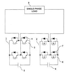
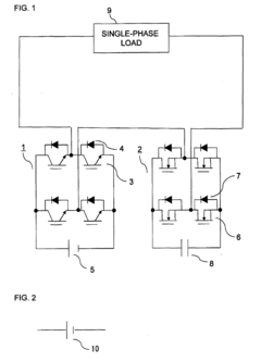
Power converting apparatus
PatentActiveUS20110089765A1
Innovation
- A power converting apparatus comprising a first inverter circuit with Si-based semiconductor devices and a second inverter circuit with non-Si-based semiconductor devices, where the AC side output terminals of both circuits are connected in series to supply AC power with a prescribed voltage waveform, allowing for varying operating conditions and reducing overall power loss.
Thermal Management Strategies for High-Frequency Power Stages
Thermal management is a critical aspect of high-frequency power stages utilizing SiC and GaN technologies. The superior switching capabilities of these wide bandgap semiconductors generate significant heat that must be effectively dissipated to maintain performance and reliability. Both SiC and GaN devices exhibit different thermal characteristics that necessitate tailored cooling strategies.
For SiC-based power stages, which typically operate at higher voltage classes (650V-1700V), thermal management often employs traditional cooling methods enhanced for higher temperature operation. SiC's ability to function at junction temperatures up to 200°C provides thermal headroom, but requires careful consideration of packaging materials and thermal interface materials (TIMs) that can withstand these elevated temperatures.
GaN devices, predominantly used in lower voltage applications (100V-650V), present unique thermal challenges due to their extremely fast switching speeds (up to 100MHz) and smaller die sizes. The concentrated heat generation in GaN devices demands more sophisticated cooling solutions, including advanced direct-cooling techniques and optimized PCB layouts with embedded heat spreading layers.
Liquid cooling systems are increasingly being adopted for high-power SiC applications, offering superior heat dissipation capabilities compared to traditional air cooling. These systems can maintain lower junction temperatures, reducing switching losses and improving overall efficiency. For GaN applications, microfluidic cooling channels integrated directly into the package are emerging as promising solutions for managing localized hotspots.
Advanced thermal interface materials play a crucial role in both technologies. Diamond-based TIMs and metal matrix composites offer thermal conductivities exceeding 1000 W/mK, significantly reducing the thermal resistance between the die and heat sink. These materials are particularly beneficial for GaN devices where thermal bottlenecks at interfaces can severely limit performance.
Dynamic thermal management strategies are also gaining traction, employing real-time temperature monitoring and adaptive control algorithms. These systems can modulate switching frequencies and gate drive parameters based on thermal conditions, optimizing the performance-temperature trade-off during operation. This approach is especially valuable for SiC devices in applications with variable load profiles.
Innovative packaging technologies, such as double-sided cooling and embedded die technologies, are being developed to address the thermal challenges of high-frequency operation. These approaches provide multiple heat dissipation paths, effectively doubling the cooling capacity compared to conventional single-sided cooling methods, and are particularly advantageous for high-power SiC modules operating at elevated switching frequencies.
Cost-Performance Trade-offs in Wide Bandgap Power Applications
When evaluating wide bandgap (WBG) semiconductors like Silicon Carbide (SiC) and Gallium Nitride (GaN) for solid-state transformer (SST) power stages, cost-performance trade-offs become a critical consideration for design engineers and system architects.
SiC devices typically command a premium price compared to GaN alternatives, with costs approximately 30-40% higher for comparable power ratings. However, this cost differential must be evaluated against SiC's superior performance in high-voltage applications exceeding 650V, where its thermal conductivity (3-4x higher than GaN) provides significant advantages in thermal management and reliability.
GaN devices offer compelling cost advantages in the 100-650V range, particularly for applications requiring high switching frequencies. The lower gate charge and output capacitance of GaN enable switching speeds 3-5 times faster than SiC counterparts, significantly reducing switching losses in high-frequency operations. This translates to smaller passive components and reduced overall system costs despite the semiconductor component itself.
The economic equation shifts dramatically when considering total system cost rather than just component pricing. SiC's higher voltage handling capability (currently commercial devices up to 1700V versus GaN's typical 650V ceiling) reduces the need for complex multi-level topologies in medium voltage applications, potentially lowering system complexity and associated costs.
Manufacturing maturity also impacts the cost-performance balance. SiC manufacturing has reached greater maturity with multiple suppliers and established supply chains, while GaN technology, particularly GaN-on-Si, continues to evolve with promising cost reduction trajectories as volumes increase and manufacturing yields improve.
Energy efficiency creates another dimension in the cost analysis. GaN's lower switching losses at high frequencies can yield 1-2% higher system efficiency in certain applications, generating significant operational cost savings over the product lifetime that may offset higher initial component costs, particularly in applications with continuous operation.
The optimal cost-performance balance ultimately depends on specific application requirements. For high-voltage, high-temperature applications with moderate switching frequencies, SiC often provides better long-term value despite higher initial costs. Conversely, GaN typically offers superior economics for lower voltage, high-frequency applications where switching performance dominates the system design considerations.
Unlock deeper insights with Patsnap Eureka Quick Research — get a full tech report to explore trends and direct your research. Try now!
Generate Your Research Report Instantly with AI Agent
Supercharge your innovation with Patsnap Eureka AI Agent Platform!