How to Specify Gate Drivers & Isolation for MV SiC — Timing & Protection
AUG 28, 20259 MIN READ
Generate Your Research Report Instantly with AI Agent
Patsnap Eureka helps you evaluate technical feasibility & market potential.
SiC Gate Driver Technology Background and Objectives
Silicon Carbide (SiC) power devices have emerged as revolutionary components in power electronics over the past two decades, offering superior performance characteristics compared to traditional silicon-based semiconductors. The evolution of SiC technology has been marked by significant improvements in material quality, device design, and manufacturing processes, enabling higher voltage ratings, lower switching losses, and higher temperature operation capabilities.
The development trajectory of SiC power devices began in the early 2000s with relatively simple structures and limited commercial availability. By the 2010s, SiC MOSFETs and Schottky diodes had entered mainstream markets, primarily in lower voltage applications. Recent years have witnessed the expansion of SiC technology into medium voltage (1.7kV to 10kV) applications, opening new possibilities for power conversion systems in industrial drives, renewable energy, and grid infrastructure.
This technological progression has created unique challenges for gate driver technology, which must evolve in parallel to fully leverage SiC advantages. Traditional gate driver solutions designed for silicon IGBTs are inadequate for medium voltage SiC devices due to fundamentally different switching characteristics, higher dv/dt and di/dt rates, and more stringent protection requirements.
The primary objective of this technical research is to establish comprehensive specifications for gate drivers and isolation technologies specifically optimized for medium voltage SiC power devices. We aim to identify critical timing parameters that ensure optimal switching performance while preventing potentially destructive conditions such as shoot-through and voltage overshoot. Additionally, we seek to define protection mechanisms capable of responding within nanosecond timeframes to safeguard these expensive semiconductor devices.
A secondary goal is to evaluate isolation technologies that can maintain signal integrity across the high potential barriers present in medium voltage applications while withstanding the extreme dv/dt conditions inherent to SiC switching. This includes assessment of various isolation methods including optical, magnetic, and capacitive approaches, with particular attention to their long-term reliability under harsh operating conditions.
The ultimate technical target is to develop design guidelines that enable power electronics engineers to properly specify gate driver requirements for medium voltage SiC applications, balancing performance optimization with system reliability and protection. These specifications must address the unique challenges of SiC technology while remaining practical for implementation in commercial and industrial power conversion systems.
Market Demand Analysis for Medium Voltage SiC Applications
The medium voltage Silicon Carbide (SiC) device market is experiencing significant growth driven by increasing demands for higher efficiency, power density, and reliability in power conversion systems. Current market analysis indicates that the global SiC power semiconductor market is projected to grow at a compound annual growth rate of 29% through 2026, with medium voltage applications representing a substantial portion of this expansion.
Industrial sectors are the primary drivers of demand for medium voltage SiC applications, particularly in renewable energy integration, industrial motor drives, traction systems, and grid infrastructure. The renewable energy sector specifically shows strong demand as countries worldwide accelerate their transition to clean energy sources, requiring more efficient power conversion solutions for solar inverters, wind power converters, and energy storage systems.
Electric vehicle (EV) charging infrastructure represents another significant market segment, with the rapid deployment of fast and ultra-fast charging stations necessitating medium voltage SiC devices that can handle higher power levels while maintaining efficiency. The automotive sector itself is gradually adopting medium voltage architectures for electric powertrains in commercial vehicles, creating additional demand for SiC technology.
Data centers and telecommunications infrastructure are emerging as important markets for medium voltage SiC applications, driven by the need for more efficient power distribution systems and uninterruptible power supplies. These facilities require solutions that can reduce energy consumption while handling increasing power demands, making SiC devices particularly attractive.
Market research indicates that end-users are primarily concerned with several key performance factors when considering medium voltage SiC solutions. These include switching speed capabilities, thermal performance, reliability under high-voltage stress conditions, and comprehensive protection features. The timing requirements for gate drivers have become increasingly critical as switching frequencies increase, with customers demanding precise control to maximize efficiency while preventing damaging conditions.
Regional analysis shows that Asia-Pacific currently leads in medium voltage SiC adoption, followed by North America and Europe. China, Japan, and South Korea are making substantial investments in SiC manufacturing capacity, while European markets are driven by stringent efficiency regulations and renewable energy targets.
The market is also witnessing increased demand for integrated solutions that combine SiC devices with optimized gate drivers and isolation technologies, as customers seek to reduce design complexity and accelerate time-to-market. This trend is particularly evident in medium voltage applications where system reliability and protection requirements are more stringent than in low-voltage scenarios.
Current Challenges in SiC Gate Driver Isolation
Silicon Carbide (SiC) power devices have emerged as a revolutionary technology in medium voltage applications, offering superior performance compared to traditional silicon-based solutions. However, the isolation requirements for SiC gate drivers present significant technical challenges that must be addressed to fully leverage the benefits of this technology.
One of the primary challenges in SiC gate driver isolation is the significantly higher switching speeds compared to silicon devices. SiC MOSFETs and JFETs can switch at rates exceeding 100 V/ns, which creates substantial common-mode transients that can compromise isolation barriers. These high dv/dt rates generate displacement currents through parasitic capacitances in isolation components, potentially causing false triggering or damage to control circuitry.
The higher operating voltages of medium voltage SiC applications (typically 1.7kV to 10kV) demand isolation solutions with exceptional dielectric strength and long-term reliability. Traditional optocoupler-based isolation struggles to maintain performance at these voltage levels while meeting the lifetime requirements of industrial applications. The degradation of optical components over time becomes a critical concern in harsh operating environments.
Temperature stability presents another significant challenge. SiC devices can operate at junction temperatures up to 200°C, requiring isolation components that maintain their electrical characteristics across extreme temperature ranges. Many conventional isolation technologies exhibit significant parameter drift at elevated temperatures, affecting timing precision and protection response.
The timing requirements for SiC gate drivers are exceptionally stringent. Propagation delay and pulse width distortion must be minimized to maintain switching efficiency and prevent shoot-through conditions. The isolation barrier introduces inherent delays that must be carefully managed, particularly in half-bridge and multi-level converter topologies where precise timing coordination between multiple drivers is essential.
Common-mode transient immunity (CMTI) has become a critical specification for SiC gate driver isolation. While silicon applications typically require CMTI ratings of 25-50 kV/μs, medium voltage SiC applications often demand CMTI capabilities exceeding 100 kV/μs. Few isolation technologies can reliably achieve these levels while maintaining other performance parameters.
Protection mechanisms must operate with extremely low latency across the isolation barrier. Conventional approaches that rely on detecting fault conditions and then communicating across isolation boundaries often cannot respond quickly enough to prevent device failure in SiC systems. This necessitates new approaches to integrated protection that can act within nanoseconds rather than microseconds.
Power transfer across the isolation barrier represents another significant challenge. SiC gate drivers typically require higher gate drive voltages (±15V to ±20V) and peak currents compared to silicon counterparts, placing additional demands on isolated power supplies that must maintain efficiency while preserving isolation integrity.
Current Gate Driver Timing and Protection Methodologies
01 Isolation techniques for SiC gate drivers
Various isolation techniques are employed in gate drivers for SiC devices to ensure safe operation at medium voltage levels. These include optical isolation, transformer-based isolation, and capacitive isolation methods that provide electrical separation between control circuits and power stages. These isolation barriers protect low-voltage control circuitry while enabling reliable switching of high-voltage SiC devices, with particular attention to maintaining signal integrity across the isolation boundary.- Isolation techniques for SiC gate drivers: Various isolation techniques are employed in gate drivers for medium voltage SiC devices to ensure safe operation and prevent damage from high voltage transients. These include optical isolation, transformer-based isolation, and capacitive isolation methods that provide galvanic separation between control circuits and power stages while maintaining signal integrity. Proper isolation is critical for protecting control circuitry and ensuring reliable operation in medium voltage applications.
- Timing control and synchronization for SiC gate drivers: Precise timing control is essential for SiC gate drivers to ensure optimal switching performance and prevent shoot-through conditions. Advanced timing control mechanisms include dead-time insertion circuits, propagation delay compensation, and synchronization techniques that coordinate multiple gate drivers in complex power conversion systems. These timing control features help maximize efficiency while protecting the SiC devices from damage due to improper switching sequences.
- Protection circuits for MV SiC devices: Protection circuits are integrated into gate drivers to safeguard SiC devices from overcurrent, overvoltage, and thermal events. These circuits include fast-acting fault detection mechanisms, soft shutdown capabilities, and active clamping techniques that respond to abnormal operating conditions. Advanced protection schemes monitor multiple parameters simultaneously and implement coordinated responses to prevent catastrophic failures in medium voltage applications.
- Gate driver integration and packaging for SiC applications: Specialized integration and packaging solutions are developed for SiC gate drivers to address thermal management, noise immunity, and size constraints. These include multi-chip modules, integrated power modules with embedded gate drivers, and advanced thermal interface materials that optimize heat dissipation. Compact packaging designs reduce parasitic inductances and improve switching performance while maintaining isolation requirements for medium voltage applications.
- Advanced control algorithms for SiC gate drivers: Sophisticated control algorithms enhance the performance of SiC gate drivers by optimizing switching trajectories, implementing adaptive gate drive techniques, and providing intelligent protection functions. These algorithms can adjust gate drive parameters based on operating conditions, implement active gate driving to control switching speed, and provide predictive protection based on device behavior analysis. Such advanced control methods maximize the benefits of SiC technology while ensuring reliable operation in medium voltage applications.
02 Timing control and dead-time management
Precise timing control is critical for SiC gate drivers in medium voltage applications to prevent shoot-through conditions. Advanced timing circuits manage the turn-on and turn-off sequences with appropriate dead-time insertion between switching transitions. These timing control mechanisms ensure safe operation by preventing simultaneous conduction of high-side and low-side devices while optimizing switching performance to take advantage of SiC's fast switching capabilities.Expand Specific Solutions03 Protection circuits for SiC devices
Protection circuits are integrated into gate drivers to safeguard SiC devices from overcurrent, overvoltage, and thermal events. These circuits include fast-acting short-circuit protection, desaturation detection, and active clamping mechanisms that respond within nanoseconds to prevent device failure. The protection systems monitor critical parameters and implement controlled shutdown procedures when fault conditions are detected, extending the operational lifetime of SiC devices in medium voltage applications.Expand Specific Solutions04 Gate drive power supply and bootstrapping techniques
Specialized power supply configurations are required for medium voltage SiC gate drivers, particularly for floating high-side drivers. Bootstrapping circuits, isolated DC-DC converters, and charge pump mechanisms provide the necessary gate drive voltage while maintaining isolation. These power supply solutions ensure stable gate voltage levels during high-frequency switching operations and under varying load conditions, which is essential for optimal SiC device performance.Expand Specific Solutions05 Integration and packaging for high-temperature operation
Advanced integration and packaging techniques address the thermal challenges associated with SiC devices in medium voltage applications. These include high-temperature compatible materials, thermally optimized layouts, and integrated cooling solutions that maintain gate driver functionality at elevated temperatures. The packaging approaches also focus on minimizing parasitic inductances and capacitances to fully leverage the high-speed switching capabilities of SiC devices while ensuring reliable operation in harsh environments.Expand Specific Solutions
Key Industry Players in SiC Gate Driver Solutions
The medium voltage Silicon Carbide (SiC) device market is currently in a growth phase, with increasing adoption across power electronics applications. The market size is expanding rapidly, projected to reach significant value as industries transition from traditional silicon to SiC technology for higher efficiency and performance. Technologically, SiC gate drivers and isolation solutions are advancing toward maturity, with key players like Infineon Technologies, Microchip Technology, and ROHM leading innovation in timing precision and protection mechanisms. Major automotive manufacturers including Toyota, Nissan, and DENSO are driving adoption through electric vehicle applications, while power infrastructure companies such as Mitsubishi Electric, Fuji Electric, and State Grid are implementing SiC in grid applications. Research institutions like Purdue and University of Houston continue advancing fundamental technologies, creating a competitive landscape balanced between established semiconductor leaders and specialized SiC-focused entrants.
Mitsubishi Electric Corp.
Technical Solution: Mitsubishi Electric has developed integrated gate driver solutions optimized for their SiC power modules in medium voltage applications. Their VLA500-01R gate driver employs a hybrid isolation approach combining optical signal transmission with isolated power supply, achieving isolation voltages up to 4kV and CMTI performance exceeding 100 kV/μs. The driver implements precise timing control with propagation delays under 120ns and channel-to-channel matching within 15ns. For protection, Mitsubishi's solution features a multi-tiered approach with primary short-circuit detection based on desaturation monitoring (response time <2μs) and secondary protection through gate voltage monitoring. Their Advanced Active Gate Control technology dynamically adjusts gate drive parameters based on operating conditions, with particular focus on managing the Miller effect during fast switching transitions. The driver incorporates temperature-dependent gate voltage compensation to maintain consistent switching performance across the operating temperature range. Mitsubishi's latest generation includes built-in monitoring and diagnostic capabilities with isolated feedback channels for system-level protection coordination[7][9].
Strengths: Optimized specifically for Mitsubishi's SiC power modules ensuring compatibility; robust design with proven reliability in industrial applications; comprehensive application support. Weaknesses: Limited flexibility for use with third-party power devices; relatively higher cost; larger physical footprint compared to more integrated solutions.
Microchip Technology, Inc.
Technical Solution: Microchip has developed the AgileSwitch® gate driver technology specifically addressing the timing and protection challenges of medium voltage SiC devices. Their solution features Augmented Switching™ technology that provides programmable gate drive profiles with up to 9 distinct segments during turn-on and turn-off transitions. This allows precise control of dv/dt and di/dt to minimize ringing and EMI while optimizing switching losses. For isolation, Microchip employs reinforced digital isolators with 1500V working voltage and CMTI ratings exceeding 100 kV/μs. The protection architecture includes configurable desaturation detection with response times under 2μs and Adaptive Short Circuit Response™ that modulates the turn-off profile during fault conditions to minimize voltage overshoots. Their drivers feature temperature-compensated timing control that maintains consistent propagation delays (±5ns) across the operating temperature range. The SP6LI product family incorporates SiC-specific protection features including gate voltage monitoring and Miller current suppression with adjustable thresholds[4][6].
Strengths: Highly configurable gate drive profiles allowing application-specific optimization; comprehensive development environment with GUI-based configuration tools; field-programmable protection parameters. Weaknesses: Higher complexity requiring more engineering resources for implementation; larger footprint compared to simpler solutions; higher power consumption due to advanced features.
Critical Patents and Innovations in SiC Driver Isolation
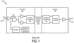
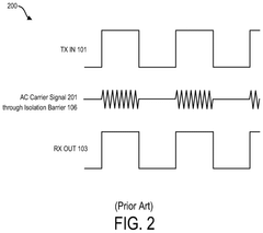
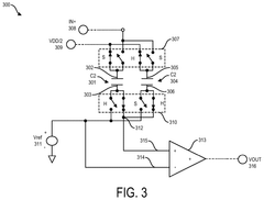
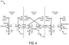
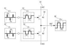
Silicon Carbide Driver Using High Voltage Capacitors for Isolation and Signal Transmission
PatentPendingUS20250183890A1
Innovation
- A gate driver circuit is designed with a first and second capacitor, each with terminals that are selectively coupled to an input drive signal and a power supply voltage using high voltage domain switches, and to a reference voltage and high impedance node using low voltage domain switches. A comparator compares the reference voltage with the voltage at the high impedance node to generate an output drive signal, effectively transferring the high voltage input drive signal to a low voltage output drive signal.
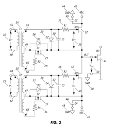
High temperature operation silicon carbide gate driver
PatentInactiveUS20130063184A1
Innovation
- A gate driver circuit utilizing silicon on insulator (SOI) and SiC devices with high-temperature passive components, including transformers, diodes, and capacitors, operating from -70°C to 250°C and 100 kHz to 500 kHz, capable of sinking/source currents up to 25 Amperes, and providing electrical isolation and dv/dt noise minimization.
Thermal Management Considerations for SiC Gate Drivers
Thermal management is a critical aspect of SiC gate driver design due to the high switching frequencies and power densities characteristic of SiC devices. The gate driver's thermal performance directly impacts the reliability and operational stability of medium voltage SiC power systems. Effective thermal management strategies must address both the heat generated within the gate driver circuit itself and the thermal coupling from the SiC power device.
The primary heat sources in gate driver circuits include the output stage transistors, isolated DC-DC converters, and protection circuitry. These components experience significant thermal stress during high-frequency switching operations typical in SiC applications. Temperature rise in these components can lead to timing variations, threshold voltage shifts, and ultimately impact the precise control required for medium voltage SiC devices.
Gate driver ICs for SiC applications typically operate within a temperature range of -40°C to 125°C, with some specialized versions extending to 150°C. However, maintaining operation below 100°C is recommended to ensure optimal timing characteristics and long-term reliability. This becomes particularly challenging in medium voltage applications where isolation barriers must maintain their integrity under elevated temperatures.
Thermal coupling between the SiC power device and gate driver requires careful consideration in layout design. Physical separation, thermal barriers, and strategic component placement can minimize heat transfer from the power device to sensitive gate driver components. The isolation components, crucial for medium voltage applications, are particularly susceptible to thermal stress and require adequate thermal management to maintain their isolation properties over time.
Cooling solutions for gate driver circuits range from passive techniques such as heat sinks and thermal vias to active methods including forced air cooling. The selection depends on the application's power density, environmental conditions, and reliability requirements. For medium voltage applications, where safety is paramount, redundant cooling strategies may be necessary to ensure the gate driver's thermal stability under all operating conditions.
Temperature monitoring and protection features should be integrated into the gate driver design to prevent thermal runaway scenarios. These may include temperature sensors with feedback to control circuits, automatic derating of switching frequency at elevated temperatures, and thermal shutdown capabilities. Such features are essential for protecting both the gate driver and the expensive SiC power devices in medium voltage systems.
The thermal design must also account for transient thermal events, such as short-circuit conditions, where the gate driver may need to handle significant power dissipation for brief periods. The thermal time constants of various components and materials in the gate driver assembly determine the system's ability to withstand these transient events without compromising the timing precision required for SiC device protection.
EMI/EMC Compliance Standards for Medium Voltage Applications
Medium voltage SiC applications must adhere to stringent EMI/EMC compliance standards to ensure operational safety and reliability. The International Electrotechnical Commission (IEC) provides the primary framework through standards like IEC 61000 series, which addresses electromagnetic compatibility requirements for industrial environments. Specifically, IEC 61000-4-4 covers electrical fast transient/burst immunity, critical for gate driver circuits in medium voltage applications.
For medium voltage SiC devices, the EN 55011/CISPR 11 standards are particularly relevant, classifying industrial equipment into Groups 1 and 2 with corresponding emission limits. SiC power converters typically fall under Class A (industrial) or Class B (residential) categories, with Class B imposing stricter emission limits.
The rapid switching capabilities of SiC devices (10-100 ns) generate significant electromagnetic interference, necessitating compliance with IEC 61800-3 for variable speed drive systems. This standard defines four categories (C1-C4) based on installation environment and voltage level, with medium voltage SiC applications typically falling under C3 or C4 categories.
UL 1741 and IEEE 1547 standards are essential for grid-connected applications, specifying requirements for inverters and interconnection systems. These standards address isolation requirements and protection mechanisms that directly impact gate driver design for medium voltage SiC devices.
Regional variations in EMC standards must also be considered. While European markets follow the CE marking requirements based on the EMC Directive 2014/30/EU, North American markets adhere to FCC Part 15 regulations, and Asian markets may have country-specific requirements such as Japan's VCCI or China's CCC certification.
Testing methodologies for EMI/EMC compliance include conducted emissions testing (0.15-30 MHz), radiated emissions testing (30 MHz-1 GHz), and immunity testing against electrostatic discharge, radiated fields, and electrical fast transients. For medium voltage SiC applications, special attention must be paid to common-mode currents and dv/dt effects that can compromise isolation barriers in gate drivers.
Compliance strategies for gate driver designs include implementing proper shielding techniques, optimizing PCB layouts with ground planes, using common-mode chokes and filters, and selecting appropriate isolation technologies with high common-mode transient immunity (CMTI) ratings exceeding 100 kV/μs for medium voltage SiC applications.
Unlock deeper insights with Patsnap Eureka Quick Research — get a full tech report to explore trends and direct your research. Try now!
Generate Your Research Report Instantly with AI Agent
Supercharge your innovation with Patsnap Eureka AI Agent Platform!