

How to Optimize Circuit Layout for Half Wave Rectifiers?
JUL 15, 20259 MIN READ
Generate Your Research Report Instantly with AI Agent
PatSnap Eureka helps you evaluate technical feasibility & market potential.
Half Wave Rectifier Background and Objectives
Half-wave rectifiers have been a fundamental component in electronic circuits since the early days of radio technology. These simple yet effective devices play a crucial role in converting alternating current (AC) to pulsating direct current (DC), making them essential in various applications, from power supplies to signal processing.
The evolution of half-wave rectifiers has been closely tied to the development of semiconductor technology. Initially, vacuum tubes were used as rectifying elements, but the advent of solid-state electronics, particularly the introduction of semiconductor diodes, revolutionized the field. This transition marked a significant milestone in the miniaturization and efficiency improvement of electronic circuits.
As technology progressed, the focus shifted from merely achieving rectification to optimizing the performance and efficiency of half-wave rectifier circuits. Key areas of improvement have included reducing power losses, minimizing ripple in the output voltage, and enhancing overall circuit reliability. These advancements have been driven by the increasing demands of modern electronic devices for more efficient and compact power management solutions.
The optimization of circuit layout for half-wave rectifiers has become a critical aspect of electronic design. This focus stems from the recognition that proper layout can significantly impact the rectifier's performance, affecting factors such as power efficiency, electromagnetic interference (EMI), and thermal management. As electronic devices continue to shrink in size while demanding higher performance, the importance of optimized circuit layouts has grown exponentially.
The primary objectives in optimizing half-wave rectifier layouts include minimizing parasitic effects, reducing electromagnetic emissions, improving heat dissipation, and enhancing overall circuit stability. These goals are particularly crucial in high-frequency applications, where even small layout imperfections can lead to significant performance degradation.
Recent technological trends have further emphasized the need for advanced optimization techniques. The rise of Internet of Things (IoT) devices, wearable technology, and compact mobile electronics has created a demand for ultra-efficient, miniaturized power management solutions. In this context, half-wave rectifiers, despite their simplicity, continue to play a vital role, necessitating ongoing research and development in layout optimization.
Looking ahead, the field of half-wave rectifier optimization is expected to intersect with emerging technologies such as advanced materials science, 3D circuit design, and AI-driven layout optimization algorithms. These developments promise to push the boundaries of what's possible in terms of efficiency, size reduction, and performance enhancement in rectifier circuits.
Market Demand Analysis for Optimized Rectifiers
The market demand for optimized half-wave rectifiers has been steadily growing, driven by the increasing need for efficient power conversion in various electronic applications. As energy efficiency becomes a paramount concern across industries, the optimization of circuit layouts for half-wave rectifiers has gained significant attention from manufacturers and end-users alike.
In the consumer electronics sector, the demand for compact and energy-efficient devices has led to a surge in the adoption of optimized rectifier circuits. Smartphones, tablets, and wearable devices require power management solutions that can maximize battery life while minimizing heat generation. This has created a substantial market opportunity for optimized half-wave rectifiers that can deliver improved performance in small form factors.
The automotive industry represents another key market for optimized rectifiers. With the rapid growth of electric and hybrid vehicles, there is an increasing need for high-efficiency power conversion systems. Optimized half-wave rectifiers play a crucial role in charging systems, power distribution networks, and motor control circuits within these vehicles. The market potential in this sector is expected to expand significantly as global automotive electrification efforts accelerate.
Industrial applications also contribute to the growing demand for optimized rectifier circuits. Factory automation, robotics, and smart manufacturing systems require reliable and efficient power conversion solutions. Optimized half-wave rectifiers can help reduce energy losses, improve overall system efficiency, and enhance the longevity of industrial equipment.
The renewable energy sector presents a promising market for optimized rectifiers. Solar inverters and wind power systems rely on efficient power conversion to maximize energy yield. As the adoption of renewable energy sources continues to increase globally, the demand for high-performance rectifier circuits is expected to grow in tandem.
Market analysis indicates that the Asia-Pacific region is likely to dominate the demand for optimized rectifiers, driven by the rapid industrialization and technological advancements in countries like China, Japan, and South Korea. North America and Europe are also significant markets, with a focus on energy-efficient solutions and sustainable technologies.
The global market for power management integrated circuits, which includes optimized rectifiers, is projected to experience substantial growth in the coming years. This growth is fueled by the increasing integration of electronic systems across various industries and the ongoing push for improved energy efficiency.
As the demand for optimized half-wave rectifiers continues to rise, manufacturers are investing in research and development to create innovative circuit layouts that can deliver higher efficiency, reduced power losses, and improved thermal management. This trend is expected to drive further market expansion and technological advancements in the field of power conversion and management.
Current Challenges in Half Wave Rectifier Design
Half wave rectifiers, while simple in concept, face several challenges in modern circuit design that hinder their optimal performance. One of the primary issues is the efficiency loss due to the inherent nature of half wave rectification. Since only one half of the AC cycle is utilized, there is a significant waste of potential power, leading to lower overall efficiency compared to full wave rectifiers.
Another challenge lies in the ripple voltage produced by half wave rectifiers. The output of these circuits contains a substantial AC component, which can cause unwanted noise and interference in sensitive electronic systems. This ripple effect necessitates additional filtering components, increasing circuit complexity and potentially introducing further inefficiencies.
The choice of diode in half wave rectifier designs also presents challenges. Ideal diodes would have zero forward voltage drop and infinite reverse breakdown voltage, but real-world diodes fall short of these characteristics. The forward voltage drop of practical diodes leads to power loss and reduced efficiency, particularly in low-voltage applications where this drop becomes more significant relative to the overall voltage.
Thermal management is another critical concern in half wave rectifier design. The pulsating nature of the current flow can lead to localized heating in components, particularly the rectifying diode. This thermal stress can affect the long-term reliability of the circuit and may require additional cooling solutions, adding to the overall complexity and cost of the design.
The layout of half wave rectifier circuits also faces challenges in minimizing electromagnetic interference (EMI). The abrupt switching action of the diode can generate high-frequency noise that may propagate through the circuit and potentially interfere with nearby electronic systems. Careful consideration of component placement and PCB trace routing is necessary to mitigate these EMI issues.
Furthermore, the size constraints in modern electronic devices pose a significant challenge for half wave rectifier designs. As products become increasingly compact, there is a growing need to miniaturize rectifier circuits without compromising their performance. This miniaturization often conflicts with the need for adequate heat dissipation and the inclusion of filtering components to reduce ripple.
Lastly, the dynamic response of half wave rectifiers to varying load conditions presents a design challenge. Sudden changes in load can cause voltage fluctuations that may exceed the acceptable limits for connected devices. Designing a rectifier circuit that can maintain stable output under diverse load conditions while still optimizing for efficiency and size is a complex balancing act for engineers.
Existing Circuit Layout Optimization Techniques
01 Basic circuit layout for half-wave rectifiers
The fundamental design of half-wave rectifier circuits typically includes a single diode connected in series with the load. This configuration allows current to flow in one direction during the positive half-cycle of the AC input, while blocking current flow during the negative half-cycle. The layout may also incorporate a transformer for voltage adjustment and isolation.- Basic circuit layout for half-wave rectifiers: The fundamental design of half-wave rectifier circuits typically includes a single diode connected in series with the load. This configuration allows current to flow in one direction during the positive half-cycle of the AC input, while blocking current flow during the negative half-cycle. The layout may also include a transformer for voltage adjustment and filtering components to smooth the output.
- Improved filtering techniques: Advanced filtering methods are employed in half-wave rectifier layouts to reduce ripple and improve output quality. These may include the use of capacitors, inductors, or combinations thereof in various configurations. Some designs incorporate multiple-stage filtering to achieve better smoothing of the rectified output.
- Integration with other circuit components: Half-wave rectifier circuits are often integrated with other components to form more complex power supply systems. This can include voltage regulators, protection circuits, or additional stages of power conversion. The layout design must consider the interaction between these components to optimize performance and minimize interference.
- Miniaturization and PCB layout optimization: Modern half-wave rectifier designs focus on miniaturization and efficient PCB layout. This involves careful component placement, trace routing, and consideration of thermal management. Advanced techniques may include the use of surface-mount components, multi-layer PCBs, and automated design tools to optimize the circuit layout.
- High-frequency and high-power applications: Specialized half-wave rectifier layouts are developed for high-frequency and high-power applications. These designs may incorporate fast-recovery diodes, heat sinking solutions, and advanced magnetic components. The layout must address issues such as parasitic inductance, capacitance, and electromagnetic interference to maintain efficiency and reliability at higher frequencies or power levels.
02 Improved filtering and smoothing techniques
Enhanced half-wave rectifier layouts often incorporate filtering and smoothing components to reduce ripple in the output voltage. This may include capacitors connected in parallel with the load, or more complex LC filter networks. These additions help to produce a steadier DC output from the pulsating half-wave rectified signal.Expand Specific Solutions03 Integration with power factor correction
Advanced half-wave rectifier designs may incorporate power factor correction (PFC) circuits. These layouts aim to improve the power factor of the rectifier by shaping the input current waveform to more closely match the voltage waveform. This can involve additional switching elements and control circuitry integrated into the basic rectifier layout.Expand Specific Solutions04 Miniaturization and PCB layout optimization
Modern half-wave rectifier designs focus on optimizing the circuit layout for printed circuit board (PCB) implementation. This involves careful component placement and trace routing to minimize parasitic effects, reduce electromagnetic interference, and improve overall efficiency. Techniques may include the use of surface-mount components and multi-layer PCB designs.Expand Specific Solutions05 Integration with control and protection circuits
Advanced half-wave rectifier layouts often incorporate additional control and protection features. These may include overvoltage protection circuits, current limiting mechanisms, and feedback control loops for output regulation. The integration of these elements requires careful consideration of component placement and signal routing in the overall circuit layout.Expand Specific Solutions
Key Players in Rectifier Circuit Industry
The optimization of circuit layout for half wave rectifiers is a mature technology within the power electronics industry. The market for this technology is stable, with moderate growth driven by increasing demand for efficient power conversion in various applications. Key players in this field include Infineon Technologies AG, ROHM Co., Ltd., and Renesas Electronics Corp., who have established strong positions through continuous innovation and product development. The competitive landscape is characterized by a mix of large semiconductor manufacturers and specialized power electronics companies, with ongoing research focused on improving efficiency, reducing component size, and enhancing thermal management. As the technology evolves, there is a growing emphasis on integrating advanced materials and smart control features to meet the demands of emerging applications in renewable energy and electric vehicles.
Siemens Corp.
Technical Solution: Siemens has developed advanced circuit layout optimization techniques for half-wave rectifiers, focusing on minimizing power losses and improving efficiency. Their approach involves using sophisticated electromagnetic simulation software to analyze current distribution and optimize component placement. Siemens employs a multi-layer PCB design with carefully routed traces to reduce parasitic capacitance and inductance[1]. They have also implemented thermal management solutions, incorporating heat sinks and thermal vias to dissipate heat effectively, which is crucial for high-power applications[3]. Additionally, Siemens utilizes advanced semiconductor materials like silicon carbide (SiC) in their rectifier designs, allowing for higher switching frequencies and improved overall performance[5].
Strengths: Comprehensive electromagnetic simulation capabilities, expertise in thermal management, and use of advanced semiconductor materials. Weaknesses: Potentially higher cost due to advanced materials and complex design processes.
Infineon Technologies AG
Technical Solution: Infineon has developed a novel approach to optimizing half-wave rectifier layouts, focusing on miniaturization and efficiency. Their technique involves integrating the rectifier circuit into a single chip using their proprietary Smart Power Technology[2]. This integration includes advanced power MOSFETs and control circuitry, significantly reducing the overall footprint. Infineon's design incorporates on-chip temperature sensors and intelligent current sensing for improved reliability and protection[4]. They have also implemented advanced packaging techniques, such as copper clip technology, to enhance thermal performance and reduce parasitic inductance[6]. Furthermore, Infineon's rectifier designs feature adaptive gate drive control, which optimizes switching behavior based on load conditions, leading to improved efficiency across a wide range of operating conditions[8].
Strengths: High level of integration, advanced packaging techniques, and adaptive control features. Weaknesses: Potential limitations in customization due to the integrated nature of the design.
Core Innovations in Half Wave Rectifier Design
Rectifier circuit
PatentWO1996033418A1
Innovation
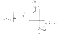
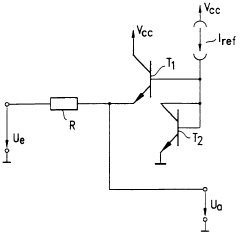
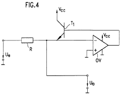
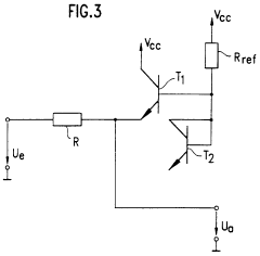
- A rectifier circuit utilizing a transistor or diode connected between a supply voltage and an input terminal, where only every second half-wave of the AC voltage is tapped at the output, allowing only half-wave rectification with minimal delay, and using a reference voltage to enable operation below threshold signal levels, which can be extended to full-wave rectification with additional components.
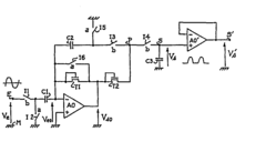
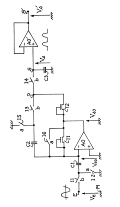
One-way rectifier with switched capacitors
PatentInactiveEP0146431A1
Innovation
- A circuit with switched capacitors, operational amplifiers, and field-effect transistors is designed, where capacitors and transistors are connected in specific phases to isolate and rectify alternating voltage, using a third capacitor to output the rectified voltage and a unity gain amplifier to maintain it without discharge, optimized for integration in MOS technology.

Thermal Management Considerations
Thermal management is a critical aspect of optimizing circuit layout for half wave rectifiers. As these circuits handle significant power levels, they generate heat that can impact performance and reliability. Effective thermal management strategies are essential to ensure optimal operation and longevity of the rectifier circuit.
One key consideration in thermal management is the selection and placement of heat sinks. Heat sinks are passive components that dissipate heat from electronic devices, particularly semiconductors like diodes used in half wave rectifiers. The design of heat sinks, including their size, shape, and material, must be carefully considered to maximize heat dissipation. Aluminum and copper are commonly used materials due to their excellent thermal conductivity. The placement of heat sinks should be strategically planned to ensure efficient heat transfer from the components generating the most heat.
Thermal interface materials (TIMs) play a crucial role in improving heat transfer between components and heat sinks. These materials, such as thermal greases, pads, or adhesives, fill microscopic air gaps between surfaces, enhancing thermal conductivity. The selection of appropriate TIMs depends on factors like thermal conductivity, ease of application, and long-term reliability.
Component placement is another vital aspect of thermal management in half wave rectifier layouts. High-power components should be positioned to allow for adequate airflow and heat dissipation. This may involve spacing components apart or arranging them in a way that promotes natural convection. In some cases, forced-air cooling through fans or blowers may be necessary for more effective heat removal.
The PCB layout itself can significantly impact thermal performance. Techniques such as using thicker copper traces for high-current paths, implementing thermal vias to conduct heat through PCB layers, and designing ground planes for better heat distribution can all contribute to improved thermal management. The choice of PCB material is also important, with materials like aluminum-core PCBs offering superior heat dissipation properties compared to standard FR-4 boards.
Temperature monitoring and protection mechanisms should be incorporated into the circuit design. This may include temperature sensors and thermal shutdown circuits to prevent damage from overheating. Such protective measures ensure the safe operation of the rectifier under various load conditions and environmental factors.
In more advanced applications, active cooling solutions may be employed. These can range from thermoelectric coolers to liquid cooling systems, depending on the specific requirements of the application. While these solutions can provide more precise temperature control, they also introduce additional complexity and cost to the design.
Ultimately, effective thermal management in half wave rectifier layouts requires a holistic approach, considering all aspects of the circuit design, component selection, and operating environment. By implementing appropriate thermal management strategies, designers can optimize the performance, reliability, and lifespan of half wave rectifier circuits.
EMC and Noise Reduction Strategies
Electromagnetic Compatibility (EMC) and noise reduction are critical considerations in optimizing circuit layout for half-wave rectifiers. These strategies aim to minimize electromagnetic interference (EMI) and improve overall system performance. A well-designed layout can significantly reduce conducted and radiated emissions, enhancing the rectifier's efficiency and reliability.
One key strategy is to minimize loop areas in the circuit layout. This involves placing components close together and using short, direct traces to connect them. By reducing the area enclosed by current-carrying conductors, the circuit becomes less susceptible to external electromagnetic fields and generates less EMI itself. For half-wave rectifiers, this principle is particularly important for the high-frequency current path between the diode and the filter capacitor.
Proper grounding techniques play a crucial role in EMC and noise reduction. Implementing a solid ground plane helps to minimize ground impedance and provides a low-impedance return path for high-frequency currents. This approach reduces common-mode noise and improves the overall EMC performance of the rectifier circuit. Additionally, separating analog and digital grounds can prevent noise coupling between different parts of the system.
Component selection and placement are also vital for EMC optimization. Using high-quality components with low parasitic inductance and capacitance can help reduce unwanted emissions. Placing filter components, such as decoupling capacitors, as close as possible to the rectifier diode and load helps to suppress high-frequency noise at its source. Furthermore, orienting components to minimize mutual coupling between circuit elements can significantly improve EMC performance.
Shielding and filtering techniques can be employed to further enhance EMC and reduce noise. Implementing proper shielding around sensitive components or the entire circuit can prevent external electromagnetic interference from affecting the rectifier's performance. Adding input and output filters, such as common-mode chokes or ferrite beads, can attenuate high-frequency noise and prevent it from propagating through the system or being emitted into the environment.
Careful consideration of PCB layout and routing is essential for effective EMC and noise reduction. Using wider traces for power-carrying conductors helps to reduce resistance and inductance, minimizing voltage drops and improving overall efficiency. Implementing guard traces or ground planes around sensitive signal lines can provide additional protection against noise coupling. Moreover, avoiding right-angle bends in traces and using curved or 45-degree angles can help reduce reflections and improve signal integrity.
By implementing these EMC and noise reduction strategies in the circuit layout of half-wave rectifiers, designers can significantly improve the overall performance, reliability, and compliance with electromagnetic compatibility standards. These techniques not only enhance the rectifier's efficiency but also contribute to the creation of more robust and interference-resistant electronic systems.
Unlock deeper insights with PatSnap Eureka Quick Research — get a full tech report to explore trends and direct your research. Try now!
Generate Your Research Report Instantly with AI Agent
Supercharge your innovation with PatSnap Eureka AI Agent Platform!