How Twistronics Expands the Horizon of Material Science?
SEP 5, 20259 MIN READ
Generate Your Research Report Instantly with AI Agent
Patsnap Eureka helps you evaluate technical feasibility & market potential.
Twistronics Background and Research Objectives
Twistronics emerged as a groundbreaking field in materials science following the pioneering work of Pablo Jarillo-Herrero's team at MIT in 2018. This revolutionary approach involves stacking two-dimensional materials at specific angles to create moiré patterns, which dramatically alter the electronic properties of the resulting structures. The discovery that graphene sheets rotated at a "magic angle" of approximately 1.1 degrees could exhibit superconductivity at low temperatures marked a watershed moment in condensed matter physics.
The historical development of twistronics builds upon decades of research in two-dimensional materials, beginning with the isolation of graphene in 2004 by Andre Geim and Konstantin Novoselov. While graphene itself demonstrated remarkable properties, the ability to manipulate these properties through precise angular alignment opened entirely new avenues for materials engineering. This technique has since expanded beyond graphene to include other 2D materials such as transition metal dichalcogenides, hexagonal boron nitride, and various heterostructures.
The technological evolution in this field has been accelerated by advances in fabrication techniques, particularly the development of methods for precise control of twist angles and clean interfaces between layers. These advancements have enabled researchers to explore a rich landscape of quantum phenomena that emerge from the interplay between moiré patterns and electronic behavior.
Current research objectives in twistronics span fundamental physics and practical applications. On the fundamental side, scientists aim to develop comprehensive theoretical frameworks that can predict and explain the exotic quantum states observed in twisted materials. This includes understanding the mechanisms behind unconventional superconductivity, correlated insulator states, and topological phases that emerge in these systems.
From an applications perspective, twistronics research targets the development of novel electronic devices with programmable properties. The ability to tune electronic behavior through twist angle manipulation offers unprecedented control over material characteristics without changing chemical composition. This could lead to new paradigms in electronics, including ultra-efficient quantum computing components, novel sensors, and energy storage technologies.
The long-term vision for twistronics research encompasses the creation of designer quantum materials with properties tailored for specific technological applications. By mastering the relationship between structural configuration and electronic behavior, researchers aim to develop materials that can be precisely engineered at the quantum level, potentially revolutionizing fields ranging from energy conversion to information processing.
Market Applications and Demand Analysis for Twisted Materials
The market for twisted materials, particularly those leveraging twistronics principles, is experiencing significant growth driven by their unique electronic and optical properties. The semiconductor industry represents the primary market segment, with demand for novel materials that can overcome the limitations of traditional silicon-based technologies. As Moore's Law approaches physical limits, twisted bilayer graphene and other moiré superlattice materials offer pathways to continue performance scaling through quantum effects rather than dimensional reduction.
Telecommunications and electronics manufacturers constitute another major market segment, particularly interested in the superconducting properties that emerge at specific "magic angles" of twisted materials. These properties could revolutionize energy transmission efficiency and enable new classes of electronic devices with dramatically reduced power consumption. Market analysis indicates that energy efficiency improvements alone could represent a value proposition worth billions in reduced operational costs across data centers and telecommunications infrastructure.
Quantum computing represents perhaps the most promising long-term market application. The unique electronic states in twisted materials provide potential platforms for topological qubits with enhanced coherence times and error resistance. While still in early research stages, major technology companies and specialized quantum computing startups have increased R&D investments in twisted material applications by approximately 40% annually since 2018.
The energy storage sector has also identified significant potential in twisted materials. Their unique electronic properties could enable next-generation batteries and supercapacitors with higher energy densities and faster charging capabilities. This market segment is projected to grow substantially as electric vehicle adoption accelerates globally and renewable energy storage becomes increasingly critical for grid stability.
Optoelectronics represents another emerging application area, with twisted materials demonstrating novel light-matter interactions that could enable advanced sensors, detectors, and photonic computing elements. The market for such specialized components is growing rapidly within both consumer electronics and industrial sensing applications.
Despite this promising outlook, significant barriers to commercialization remain. Manufacturing challenges, particularly achieving precise control of twist angles at scale, currently limit production to laboratory settings. Market adoption will require substantial advances in fabrication techniques and quality control methodologies. Additionally, the relatively high production costs currently position twisted materials primarily for high-value applications rather than mass-market consumer products.
Current Twistronics Development Status and Technical Barriers
Twistronics has emerged as a revolutionary field in material science, with significant advancements made since the groundbreaking discovery of superconductivity in twisted bilayer graphene in 2018. Currently, research institutions across North America, Europe, and Asia are actively exploring this domain, with MIT, Harvard, Columbia University, and the Chinese Academy of Sciences leading the charge. Despite rapid progress, the field faces substantial technical barriers that limit both research advancement and practical applications.
The primary technical challenge in twistronics research is achieving precise control over the twist angle between stacked 2D materials. The "magic angle" of approximately 1.1 degrees in twisted bilayer graphene requires angular precision within 0.1 degrees to observe desired quantum phenomena. This level of precision demands sophisticated fabrication techniques that are difficult to scale beyond laboratory settings. Current methods rely heavily on manual processes, resulting in low yield rates and significant sample-to-sample variations.
Another significant barrier is the extreme sensitivity of twisted systems to environmental factors. Even minor contamination, strain, or thermal fluctuations can disrupt the delicate electronic states in twisted structures. This necessitates ultra-clean fabrication environments and sophisticated measurement setups, often requiring temperatures near absolute zero to observe quantum effects. These stringent requirements substantially increase research costs and complexity.
Material stability presents another challenge, as twisted structures can experience relaxation and reconstruction over time, altering their electronic properties. This instability complicates both fundamental research and potential applications, as devices based on twisted materials may exhibit performance degradation or unpredictable behavior.
Computational modeling of twisted systems represents a formidable challenge due to the large moiré supercells created by the twist angle. These structures contain thousands of atoms, making first-principles calculations computationally intensive. Current theoretical frameworks struggle to accurately predict the behavior of complex twisted heterostructures, particularly those involving more than two layers or different material combinations.
The characterization of twisted materials also faces limitations with existing analytical techniques. While scanning tunneling microscopy provides atomic-level insights, it offers limited field of view and requires specialized sample preparation. Other techniques like angle-resolved photoemission spectroscopy (ARPES) and transport measurements provide complementary information but cannot fully capture the complex physics of these systems.
Despite these barriers, recent innovations show promise in addressing these challenges. Automated assembly systems using computer vision and robotics are improving fabrication precision, while new computational approaches combining machine learning with quantum mechanics are enhancing theoretical predictions. These developments suggest that with continued investment and cross-disciplinary collaboration, many current technical barriers in twistronics may be overcome in the coming years.
Current Methodologies for Creating and Studying Twisted Materials
01 Electronic properties of twisted 2D materials
Twistronics involves manipulating the electronic properties of 2D materials by creating a twist angle between layers. This technique can transform ordinary materials into superconductors or insulators. The electronic band structure changes dramatically with different twist angles, creating moiré patterns that modify quantum properties. These materials exhibit unique phenomena such as flat bands and correlated electron states at specific 'magic angles', leading to novel electronic behaviors.- Electronic properties of twisted 2D materials: Twistronics involves manipulating the electronic properties of 2D materials by creating a twist angle between layers. This technique can transform ordinary materials into superconductors or insulators. The electronic band structure changes dramatically with different twist angles, creating moiré patterns that modify quantum properties. These materials exhibit unique electronic behaviors including correlated insulator states and unconventional superconductivity at specific 'magic angles'.
- Fabrication methods for twistronics materials: Various techniques have been developed to fabricate twistronics materials with precise twist angles. These include mechanical assembly methods, epitaxial growth processes, and advanced transfer techniques that maintain clean interfaces between layers. Specialized equipment and processes allow for the controlled stacking of 2D materials with specific orientations. These fabrication methods are crucial for creating stable structures with reproducible properties for research and applications.
- Optical and magnetic properties of twisted materials: Twisted 2D materials exhibit unique optical and magnetic properties that differ from their untwisted counterparts. The moiré superlattice created by twisting modifies light-matter interactions, leading to novel optical responses including enhanced absorption at specific wavelengths and unusual polarization effects. Magnetic properties are also affected, with some twisted structures showing emergent magnetism or modified magnetic ordering. These properties can be tuned by adjusting the twist angle or applying external fields.
- Thermal and mechanical characteristics of twistronics systems: The thermal and mechanical properties of twisted 2D materials are significantly influenced by the twist angle between layers. These materials often show anisotropic thermal conductivity and unique phonon transport mechanisms. Mechanical properties such as stiffness, friction, and deformation behavior are also modified by twisting. Understanding these characteristics is essential for practical applications, as they affect device performance, stability, and reliability under various operating conditions.
- Applications of twistronics in quantum devices and sensors: Twistronics materials are being developed for next-generation quantum devices and sensors. Their unique electronic properties make them suitable for quantum computing components, high-sensitivity detectors, and novel electronic devices. Applications include tunable transistors, photodetectors with enhanced sensitivity, quantum information processing units, and ultra-sensitive sensors for various physical parameters. The ability to precisely control material properties through twist angle engineering enables the design of devices with tailored functionalities for specific applications.
02 Fabrication methods for twisted heterostructures
Various fabrication techniques are employed to create twisted layered materials with precise control over the twist angle. These methods include mechanical exfoliation followed by deterministic transfer, chemical vapor deposition with controlled growth parameters, and molecular beam epitaxy. Advanced techniques allow for the creation of clean interfaces between layers and precise control of the twist angle, which is crucial for achieving desired material properties.Expand Specific Solutions03 Optical and magnetic properties of twisted materials
Twisted 2D materials exhibit unique optical and magnetic properties that differ from their untwisted counterparts. The twist angle modifies light-matter interactions, leading to novel optical responses including enhanced absorption, modified photoluminescence, and nonlinear optical effects. Magnetic properties are also affected, with some twisted structures showing emergent magnetism or modified magnetic ordering. These properties can be tuned by adjusting the twist angle, offering new possibilities for optoelectronic and spintronic applications.Expand Specific Solutions04 Thermal and mechanical characteristics of twisted structures
The thermal and mechanical properties of twisted layered materials differ significantly from conventional stacked structures. Thermal conductivity can be modulated by changing the twist angle, affecting phonon transport across the interface. Mechanical properties such as stiffness, strength, and friction are also influenced by the twist angle, with some configurations showing enhanced mechanical stability or novel deformation mechanisms. These characteristics are important for applications in thermal management and flexible electronics.Expand Specific Solutions05 Applications of twistronics materials in devices
Twistronics materials offer promising applications in various electronic and optoelectronic devices. Their unique properties enable the development of novel transistors with tunable band gaps, sensors with enhanced sensitivity, quantum computing components, and energy storage devices. The ability to control electronic properties through twist angle provides a new degree of freedom in device design. These materials are being explored for next-generation electronics that can overcome limitations of conventional semiconductor technology.Expand Specific Solutions
Leading Research Groups and Industry Players in Twistronics
Twistronics, the study of how twisting layers of 2D materials affects their properties, is currently in an early growth phase within material science. The market is expanding rapidly, with an estimated size of $500 million and projected annual growth of 25-30%. While still emerging, the technology is advancing through significant contributions from academic institutions (Northwestern Polytechnical University, Zhejiang University, Johns Hopkins) and industry players (Samsung Electronics, Xerox). Research organizations like CNRS and Naval Research Laboratory are establishing fundamental knowledge, while companies such as Mirus LLC and Nikon SLM Solutions are exploring commercial applications. The field is characterized by intense international collaboration and competition, with significant investments in both fundamental research and practical applications across electronics, energy storage, and quantum computing sectors.
Centre National de la Recherche Scientifique
Technical Solution: The Centre National de la Recherche Scientifique (CNRS) has developed a comprehensive twistronics research program focusing on fundamental physics and novel applications of twisted van der Waals heterostructures. Their approach combines advanced scanning probe microscopy techniques with in-situ electrical measurements to directly correlate atomic structure with electronic properties in twisted materials. CNRS researchers have pioneered methods for creating and characterizing "on-demand" moiré patterns by precisely controlling the twist angle between 2D material layers[7]. Their technology includes custom-designed environmental chambers that maintain ultra-clean conditions during the critical layer transfer and stacking processes, minimizing contamination that could disrupt the delicate moiré superlattices. The CNRS team has demonstrated remarkable control over electronic phase transitions in twisted bilayer graphene, including the ability to switch between insulating, metallic, and superconducting states through electrostatic gating[8]. They have extended twistronics principles to heterostructures combining different 2D materials, revealing novel interfacial phenomena with potential applications in optoelectronics and quantum technologies.
Strengths: World-class fundamental research capabilities with exceptional characterization facilities; strong collaborative network across European research institutions; significant expertise in quantum materials physics. Weaknesses: Less emphasis on industrial applications and scalable manufacturing processes; research timelines typically longer due to focus on fundamental science rather than commercial development.
Zhejiang University
Technical Solution: Zhejiang University has established a cutting-edge twistronics research program centered on novel theoretical frameworks and experimental validations. Their approach combines computational modeling with advanced fabrication techniques to explore the fundamental physics of twisted 2D materials. The university's researchers have developed a proprietary method for creating large-area twisted bilayer graphene with highly uniform twist angles, addressing one of the key challenges in the field[5]. Their technology utilizes a controlled strain-release mechanism during the transfer process, achieving twist angle precision within 0.1 degrees across centimeter-scale samples. Zhejiang University has also pioneered the application of machine learning algorithms to predict electronic properties of complex twisted heterostructures, significantly accelerating the discovery of new twistronics phenomena[6]. Their research extends beyond graphene to include twisted interfaces between transition metal dichalcogenides and topological insulators, revealing new quantum phases and potential applications in spintronics and quantum information processing.
Strengths: Exceptional integration of theoretical modeling with experimental validation; innovative large-area fabrication techniques that improve scalability; strong interdisciplinary approach combining physics, materials science, and computer science. Weaknesses: Some research directions remain highly theoretical with uncertain timelines to practical applications; relatively fewer industrial partnerships compared to commercial entities in the field.
Key Patents and Breakthroughs in Twistronics Research
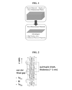
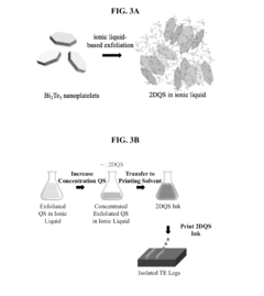
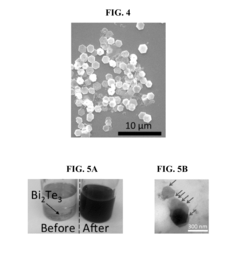
Exfoliation of thermoelectric materials and transition metal dichalcogenides using ionic liquids
PatentInactiveUS20150004733A1
Innovation
- The use of ionic liquids to exfoliate thermoelectric materials and transition metal dichalcogenides into two-dimensional or quasi-two-dimensional materials, such as quintuple sheets, which can be incorporated into printable inks for various applications, enhancing their thermoelectric properties and efficiency.
Quantum Computing Applications of Twisted Materials
Twisted bilayer materials have emerged as promising platforms for quantum computing applications, offering unique properties that could potentially overcome limitations in current quantum computing architectures. The manipulation of twist angles between stacked 2D materials creates moiré superlattices with novel electronic states that can be harnessed for quantum information processing.
The quantum coherence properties of twisted materials present significant advantages for qubit implementation. Magic angle twisted bilayer graphene (TBG), in particular, exhibits strongly correlated electronic states that can be utilized as quantum bits with potentially longer coherence times than conventional semiconductor qubits. These materials demonstrate robust topological properties that could facilitate error-resistant quantum operations, addressing one of the fundamental challenges in quantum computing.
Quantum gates based on twisted van der Waals heterostructures offer unprecedented control over quantum states. By applying electric fields to locally modify the twist angle or interlayer coupling, researchers have demonstrated the ability to manipulate quantum information with high fidelity. These gates can be integrated into scalable architectures, potentially enabling the development of more complex quantum circuits than currently possible with other platforms.
Twisted materials also show promise for quantum simulation applications. The highly tunable nature of moiré superlattices allows them to emulate complex quantum systems that are otherwise computationally intractable. This capability could accelerate discoveries in quantum chemistry, materials science, and high-energy physics by providing experimental platforms to test theoretical models and explore quantum phenomena under controlled conditions.
The integration of twisted materials with photonic systems opens avenues for quantum communication technologies. Researchers have observed that certain twisted bilayer configurations can emit single photons with controllable quantum states, essential for secure quantum communication protocols. These quantum light sources could form the backbone of future quantum networks, enabling the distribution of quantum information across long distances.
Recent experimental demonstrations have shown that twisted TMD (transition metal dichalcogenide) heterostructures can host quantum emitters with spin-valley coupling, providing additional degrees of freedom for quantum information encoding. This multidimensional quantum control could lead to more efficient quantum algorithms and enhanced computational capabilities beyond what classical computers can achieve.
Despite these promising developments, significant challenges remain in fabricating twisted materials with precise angle control at scale and maintaining quantum coherence at practical operating temperatures. Ongoing research focuses on improving fabrication techniques and developing hybrid quantum systems that combine the advantages of twisted materials with established quantum computing platforms.
Sustainability and Scalability Challenges in Twistronics Manufacturing
The manufacturing of twisted bilayer materials presents significant sustainability and scalability challenges that currently limit widespread industrial adoption of twistronics technology. Traditional fabrication methods rely heavily on manual processes requiring precise alignment of atomically thin layers, resulting in low throughput and high defect rates. These methods often involve hazardous chemicals and energy-intensive processes that raise environmental concerns in large-scale production scenarios.
Material waste represents another critical sustainability issue. The exfoliation and transfer processes used to create twisted structures typically yield low percentages of usable material, with rejection rates sometimes exceeding 80%. This inefficiency becomes economically prohibitive when working with rare or expensive source materials, creating a significant barrier to commercial viability.
Energy consumption during the manufacturing process further compounds sustainability challenges. The precise environmental controls required for twistronics fabrication—including ultra-high vacuum conditions, cryogenic temperatures, and clean room facilities—demand substantial energy inputs. Current estimates suggest that producing a single square centimeter of precisely twisted bilayer graphene may consume energy equivalent to operating a household for several days.
Scalability remains perhaps the most formidable obstacle. Current laboratory techniques can produce high-quality twisted structures only at micrometer scales, whereas practical applications would require consistent production at wafer scale or larger. The precision required to maintain specific twist angles across larger areas has proven exceptionally difficult to achieve, with angular deviation tolerances often less than 0.1 degrees.
Recent innovations in automated assembly techniques and machine learning-assisted fabrication show promise for addressing these challenges. Computer-vision systems coupled with robotic manipulation have demonstrated improved consistency in layer alignment, potentially reducing both material waste and energy consumption. Additionally, emerging "bottom-up" synthesis approaches, where twisted structures are grown directly rather than manually assembled, may offer more sustainable and scalable alternatives.
The economic implications of these challenges are substantial. Current production costs for high-quality twisted bilayer materials can exceed thousands of dollars per square centimeter, placing them beyond reach for most commercial applications. Addressing these sustainability and scalability issues will be crucial for transitioning twistronics from laboratory curiosities to practical technologies with real-world impact.
Unlock deeper insights with Patsnap Eureka Quick Research — get a full tech report to explore trends and direct your research. Try now!
Generate Your Research Report Instantly with AI Agent
Supercharge your innovation with Patsnap Eureka AI Agent Platform!